

Double density method for wirebond interconnect
a wirebond interconnect and density method technology, applied in the direction of electrical equipment, semiconductor devices, semiconductor/solid-state device details, etc., can solve the problems of increasing manufacturing costs, increasing resistance and inductance in the wire, and presenting undesirable increases in production costs
- Summary
- Abstract
- Description
- Claims
- Application Information
AI Technical Summary
Benefits of technology
Problems solved by technology
Method used
Image

Examples
Embodiment Construction
[0015] The following discussion is directed to various embodiments of the invention. Although one or more of these embodiments may be preferred, the embodiments disclosed should not be interpreted, or otherwise used, as limiting the scope of the disclosure, including the claims. In addition, one skilled in the art will understand that the following description has broad application, and the discussion of any embodiment is meant only to be exemplary of that embodiment, and not intended to intimate that the scope of the disclosure, including the claims, is limited to that embodiment.
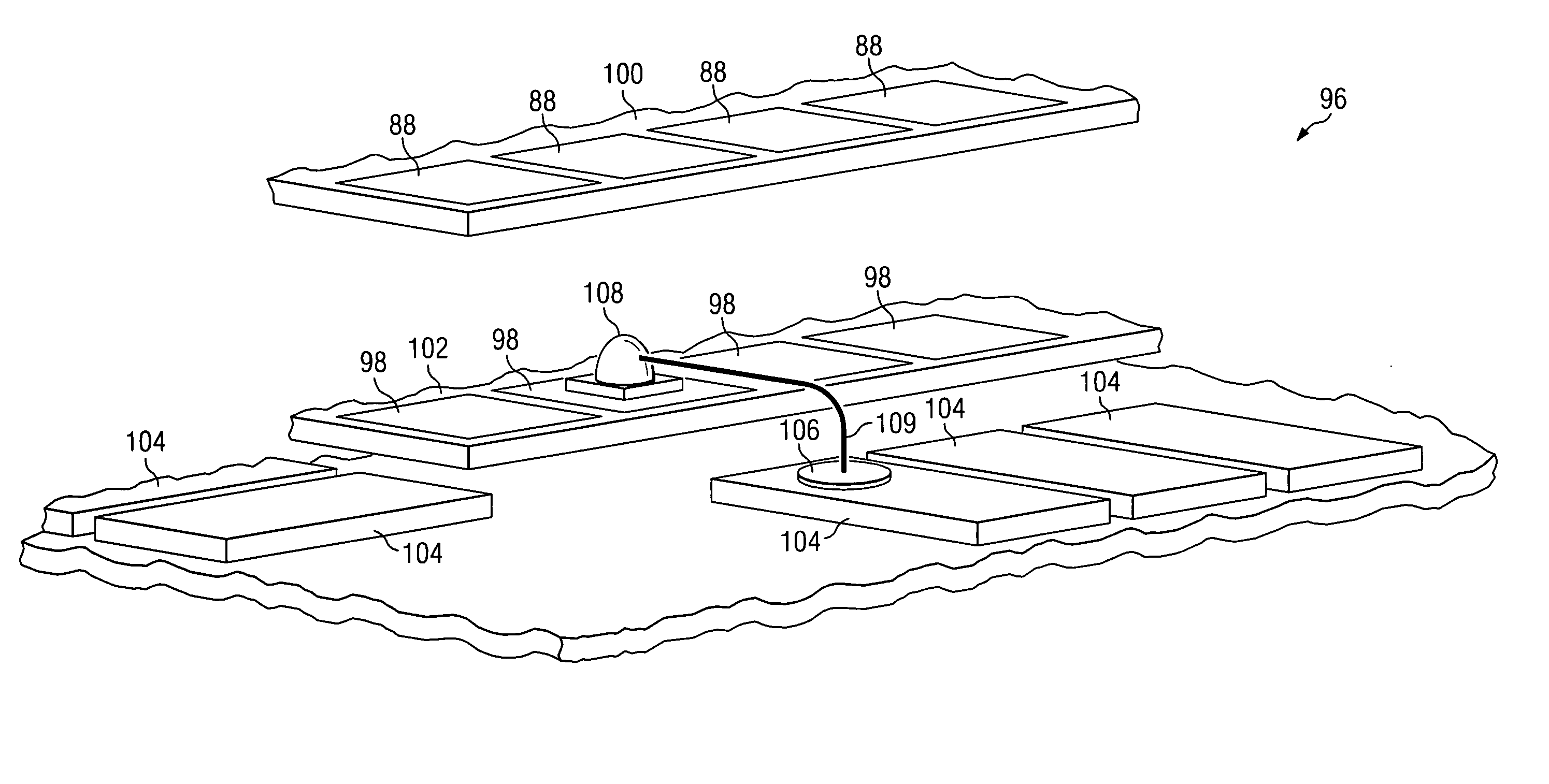
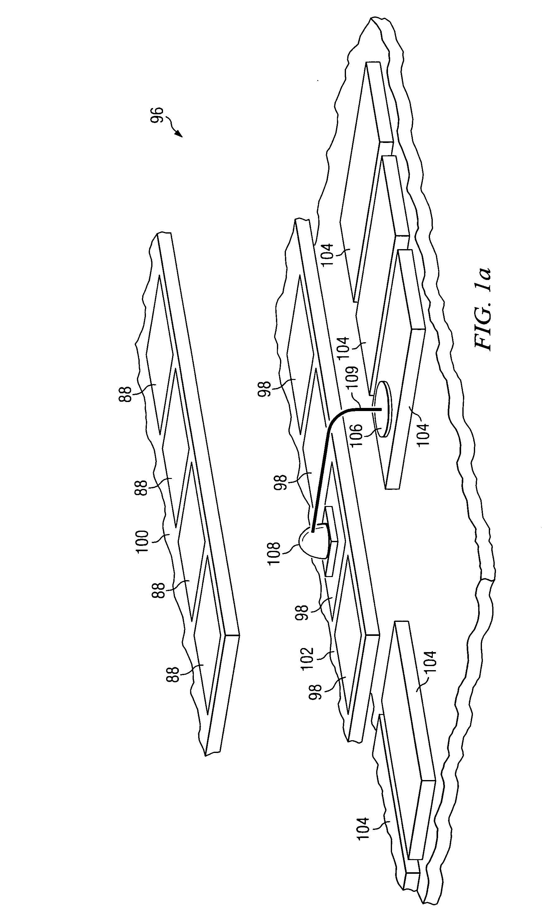
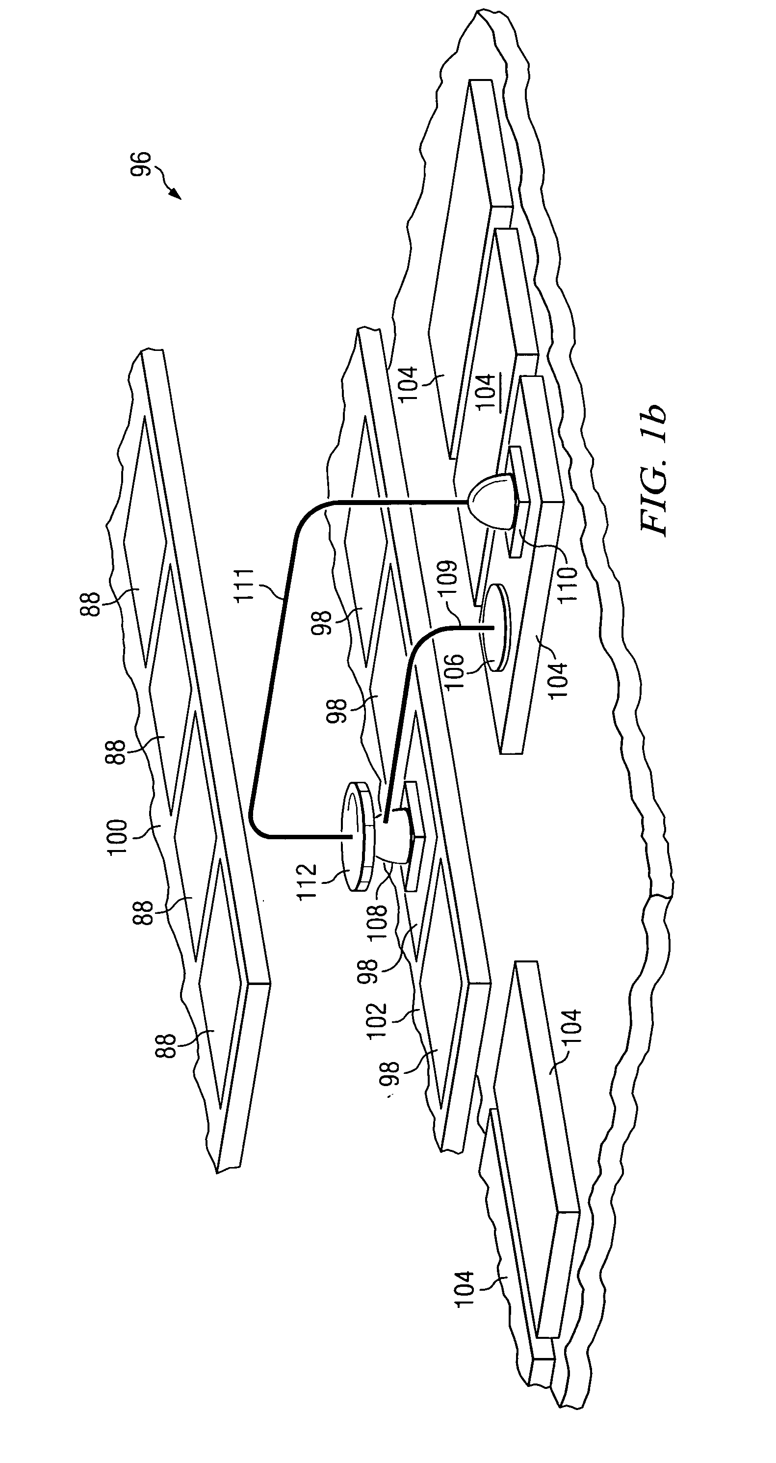
[0016] Presented herein are techniques to create multiple ball bonds atop existing bonds with minimal impact on IC reliability. These techniques increase the number of I / O connections on a die without incurring some or all of the previously mentioned difficulties. In accordance with various preferred embodiments of the invention, by using Stand Off Stitch Wirebond technology (“SSB”) (or other appropriate ...
PUM
 Abstract
Description
Claims
Application Information