Thin film transistor and flat panel display device comprising the same

a thin film transistor and flat panel display technology, applied in semiconductor devices, instruments, electrical apparatus, etc., can solve the problems of difficult patterning of semiconductor layers and degraded electrical characteristics of organic semiconductor layers

Active Publication Date: 2006-02-09
SAMSUNG DISPLAY CO LTD
View PDF1 Cites 18 Cited by
  • Summary
  • Abstract
  • Description
  • Claims
  • Application Information

AI Technical Summary

Problems solved by technology

However, in the case of an organic TFT using an organic semiconductor layer as the semiconductor layer, it is very difficult to pattern the semi...

Method used


Image

  • Thin film transistor and flat panel display device comprising the same
  • Thin film transistor and flat panel display device comprising the same
  • Thin film transistor and flat panel display device comprising the same

Examples


Embodiment Construction

[0037] Exemplary embodiments of the present invention will now be described with reference to the accompanying drawings.

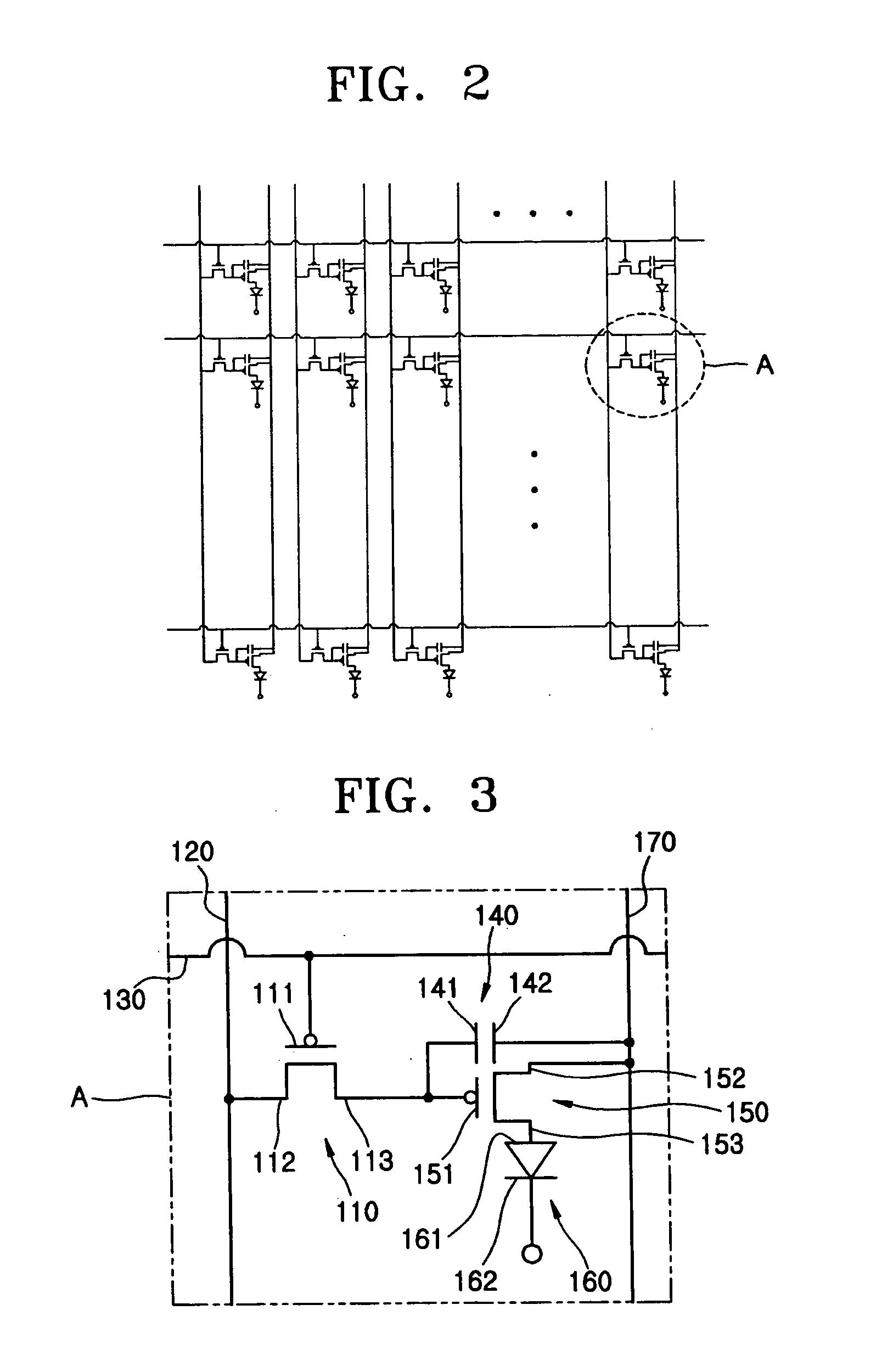
[0038] As described above, when a semiconductor layer, in particular, an organic semiconductor layer, is formed as a single body with two or more adjacent thin film transistors (TFTs), cross-talk by means of which adjacent TFTs affect one another due to leakage current and the like may occur.

[0039] In order to prevent cross-talk from occurring, the present invention proposes a flat panel display device having a thin film transistor (TFT) in which one of a source electrode and a drain electrode surrounds the other electrode in the same plane.

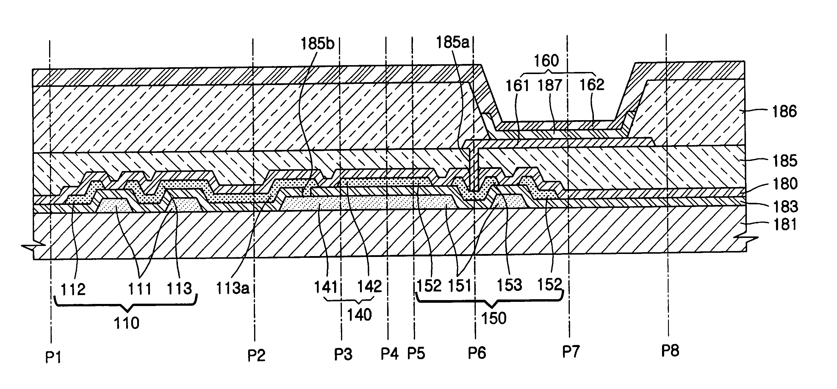
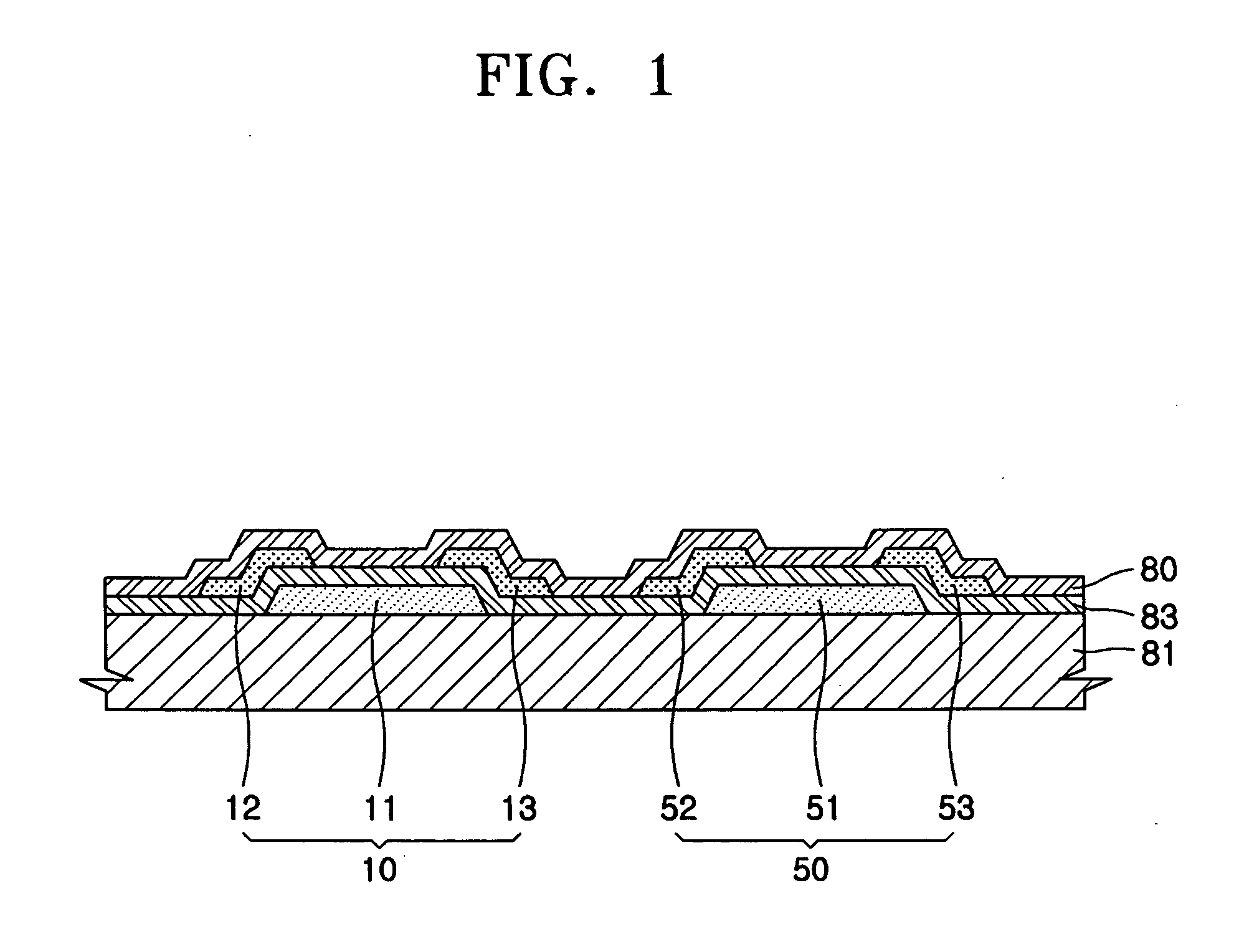
[0040]FIG. 1 is a schematic cross-sectional view of an inverted coplanar thin film transistor (TFT). Referring to FIG. 1, gate electrodes 11 and 51 are formed on a substrate 81, source electrodes 12 and 52 and drain electrodes 13 and 53 are formed above the gate electrodes 11 and 51, respectively, and a gate insulating layer ...


PUM


Abstract

In a thin film transistor and a flat panel display device having the same, cross-talk is minimized. The flat panel display device includes a substrate, a first thin film transistor, a second thin film transistor, and a display element. The first thin film transistor includes: a first gate electrode formed on the substrate; a first electrode insulated from the first gate electrode; a second electrode insulated from the first gate electrode and surrounding the first electrode in the same plane; and a first semiconductor layer insulated from the first gate electrode and contacting the first electrode and the second electrode. The second thin film transistor includes: a second gate electrode formed on the substrate and electrically connected to one of the first electrode and the second electrode; a third electrode insulated from the second gate electrode; a fourth electrode insulated from the second gate electrode and surrounding the third electrode in the same plane; and a second semiconductor layer insulated from the second gate electrode and contacting the third electrode and the fourth electrode.

Description

CLAIM OF PRIORITY [0001] This application makes reference to, incorporates the same herein, and claims all benefits accruing under 35 U.S.C. §119 earlier filed application entitled FLAT PANEL DISPLAY DEVICE, in the Korean Intellectual Property Office on Aug. 5, 2004 and there duly assigned Serial No. 10-2004-0061671. BACKGROUND OF THE INVENTION [0002] 1. Technical Field [0003] The present invention relates to a thin film transistor (TFT) and a flat panel display device comprising the same, and more particularly, to a TFT and a flat panel display device having a TFT in which cross-talk is minimized. [0004] 2. Related Art [0005] In an inverted coplanar thin film transistor (TFT), gate electrodes are formed on a substrate, source electrodes and drain electrodes are formed above the gate electrodes, and a gate insulating layer is interposed between the source electrode and the gate electrode, and between the drain electrode and the gate electrode so that the source electrodes and the dr...

Claims


Application Information

Patent Timeline
IPC IPC(8): H01L29/04
CPCH01L27/12G02F1/13624
Inventor KOO, JAE-BONKIM, KYONG-DOSUH, MIN-CHULMO, YEON-GON
Owner SAMSUNG DISPLAY CO LTD
Why Eureka
Try Eureka