Flat panel display device

a display device and flat panel technology, applied in the direction of semiconductor devices, basic electric elements, electrical apparatus, etc., can solve the problems of difficult patterning of semiconductor layers and degraded electrical characteristics of organic semiconductor layers, and achieve the effect of minimizing cross-talk

Active Publication Date: 2007-10-09
SAMSUNG DISPLAY CO LTD
View PDF8 Cites 18 Cited by
  • Summary
  • Abstract
  • Description
  • Claims
  • Application Information

AI Technical Summary

Benefits of technology

[0007]It is therefore, an object of the present invention to provide a flat panel display device having a transistor in which cross-talk is minimized.
[0008]It is another object of the present invention to provide a flat panel display device having a transistor that has a structure with connections being more simplified, better quality and more secure.
[0009]It is still another object of the present invention to provide a flat panel display device having a transistor that has a structure that is easy to implement, more efficient and yet avoids interference.

Problems solved by technology

However, in the case of an organic TFT using an organic semiconductor layer as the semiconductor layer, it is very difficult to pattern the semiconductor layer, and even if the organic semiconductor layer is patterned, electrical characteristics of the organic semiconductor layer are degraded.

Method used


Image

  • Flat panel display device
  • Flat panel display device
  • Flat panel display device

Examples


Embodiment Construction

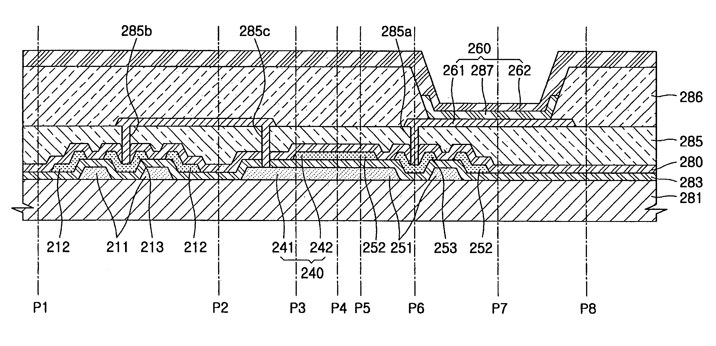
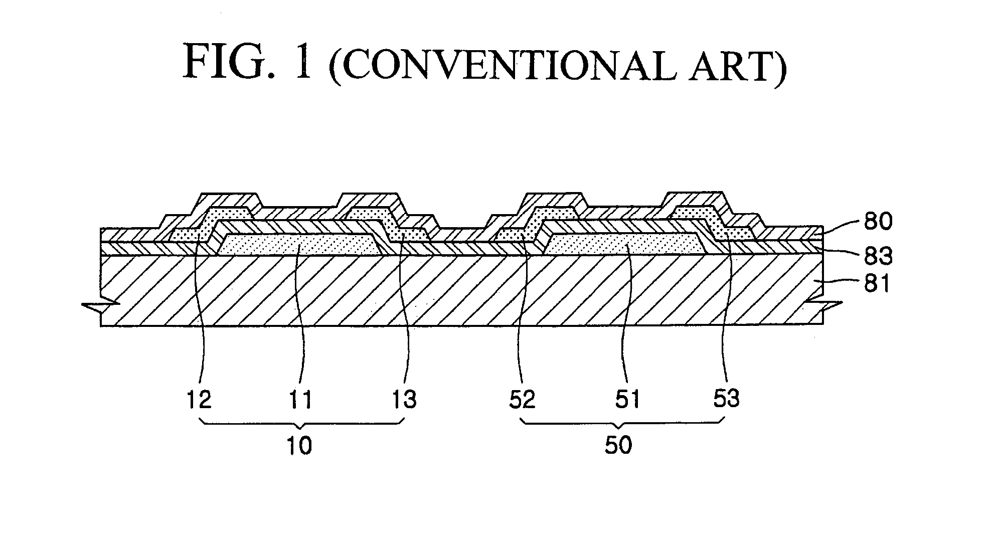
[0049]Turning now to the drawings, FIG. 1 is a schematic cross-sectional view of a conventional inverted coplanar thin film transistor (TFT). Referring to FIG. 1, gate electrodes 11 and 51 are formed on a substrate 81, source electrodes 12 and 52 and drain electrodes 13 and 53 are formed above the gate electrodes 11 and 51, respectively, and a gate insulating layer 83 is interposed between the source electrode 12 and the gate electrode 11, between the drain electrode 13 and the gate electrode 11, between the source electrode 52 and the gate electrode 51, and between the drain electrode 53 and the gate electrode 51. A semiconductor layer 80 contacts the source electrodes 12 and 52 and the drain electrodes 13 and 53. The source electrodes 12 and 52 and the drain electrodes 13 and 53 may be interchanged.

[0050]In the above structure, the semiconductor layer 80 is not patterned but is formed as a single body for two adjacent thin film transistors (TFTs) 10 and 50. In this case, cross-tal...


PUM


Abstract

A flat panel display device has a transistor in which cross-talk is minimized. The flat panel display device includes a substrate, a first gate electrode formed on the substrate, a first electrode insulated from the first gate electrode, a second electrode insulated from the first gate electrode and surrounding the first electrode in the same plane, a semiconductor layer insulated from the first gate electrode and contacting the first electrode and the second electrode, and a display element including a pixel electrode electrically connected to one of the first electrode and the second electrode.

Description

CLAIM OF PRIORITY[0001]This application makes reference to, incorporates the same herein, and claims all benefits accruing under 35 U.S.C. §119 from an application for FLAT PANEL DISPLAY DEVICE earlier filed in the Korean Intellectual Property Office on 6 Aug. 2004 and there duly assigned Serial No. 10-2004-0061947.BACKGROUND OF THE INVENTION[0002]1. Field of the Invention[0003]The present invention relates to a flat panel display device, and more particularly, to a flat panel display device having a transistor in which cross-talk is minimized.[0004]2. Description of the Related Art[0005]A conventional inverted coplanar thin film transistor (TFT), includes gate electrodes being formed on a substrate, source electrodes and drain electrodes being formed above the gate electrodes, respectively, and a gate insulating layer being interposed between the source electrode and the gate electrode, between the drain electrode and the gate electrode, between the source electrode and the gate el...

Claims


Application Information

Patent Timeline
Patent Type & Authority Patents(United States)
IPC IPC(8): H01L29/04
CPCH01L27/3262H01L27/124H01L27/3276H10K59/1213H10K59/131H01L27/12H01L27/1214
Inventor KOO, JAE-BONSUH, MIN-CHUL
Owner SAMSUNG DISPLAY CO LTD
Why Eureka
Try Eureka