Apparatus and method to reduce signal cross-talk

a technology of electromagnetic interference and signal cross-talk, applied in the field of electromagnetic interference interference, can solve the problems of increasing the size of the package, and achieve the effects of reducing cross-talk, increasing the size of the package, and reducing the cross-talk

Inactive Publication Date: 2006-05-02
INT BUSINESS MASCH CORP
View PDF10 Cites 8 Cited by
  • Summary
  • Abstract
  • Description
  • Claims
  • Application Information

AI Technical Summary

Benefits of technology

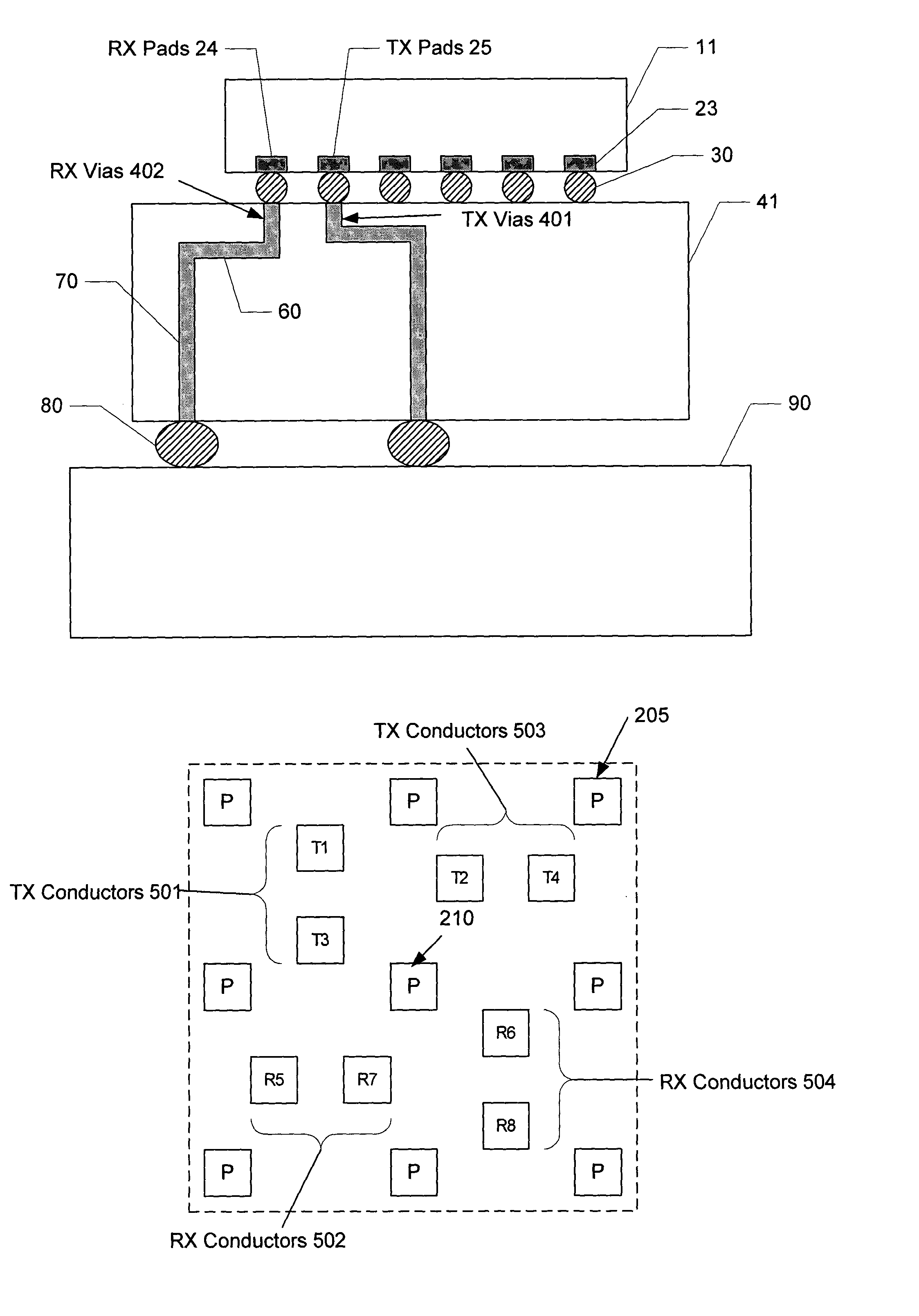
[0011]A semiconductor chip package with reduced cross-talk between adjacent signals in a layer of a carrier is disclosed. A first pair of conductors for carrying a first signal is provided in a layer of the carrier. A second pair of conductors for carrying a second signal is provided adjacent to the first pair of conductors in the layer, where the first and second pairs of conductors are configured such that cross-talk between the first and second pairs of conductors is substantially minimized, without increasing the size of the package. The height of the first pair of conductors is shorter than the second pair of conductors. Alternatively, the first and second pairs of conductors are configured so that they evenly affect each other. The chip package thus reduces the cross-talk without compromising the density of the interconnections in the package or resulting in an increase in the size of the package.

Problems solved by technology

The chip package thus reduces the cross-talk without compromising the density of the interconnections in the package or resulting in an increase in the size of the package.

Method used


Image

  • Apparatus and method to reduce signal cross-talk
  • Apparatus and method to reduce signal cross-talk
  • Apparatus and method to reduce signal cross-talk

Examples


Embodiment Construction

[0020]The present invention provides an improved apparatus and method for reducing cross-talk between adjacent signals in a layer of a semiconductor chip package. The following description is presented to enable one of ordinary skill in the art to make and use the invention and is provided in the context of a patent application and its requirements. Various modifications to the preferred embodiment will be readily apparent to those skilled in the art and the generic principles herein may be applied to other embodiments. Thus, the present invention is not intended to be limited to the embodiment shown but is to be accorded the widest scope consistent with the principles and features described herein.

[0021]To more particularly describe the features of the present invention, please refer to FIGS. 3 through 8 in conjunction with the discussion below.

[0022]FIG. 3 is a flowchart illustrating a preferred embodiment of a method for reducing cross-talk between adjacent signals in a layer of ...


PUM


Abstract

A semiconductor chip package with reduced cross-talk between adjacent signals in a layer of a carrier is disclosed. A first pair of conductors for carrying a first signal is provided in a layer of the carrier. A second pair of conductors for carrying a second signal is provided adjacent to the first pair of conductors in the layer, where the first and second pairs of conductors are configured such that cross-talk between the first and second pairs of conductors is substantially minimized, without increasing the size of the package. The height of the first pair of conductors is shorter than the second pair of conductors. Alternatively, the first and second pairs of conductors are configured so that they evenly affect each other. The chip package thus reduces the cross-talk without compromising the density of the interconnections in the package or resulting in an increase in the size of the package.

Description

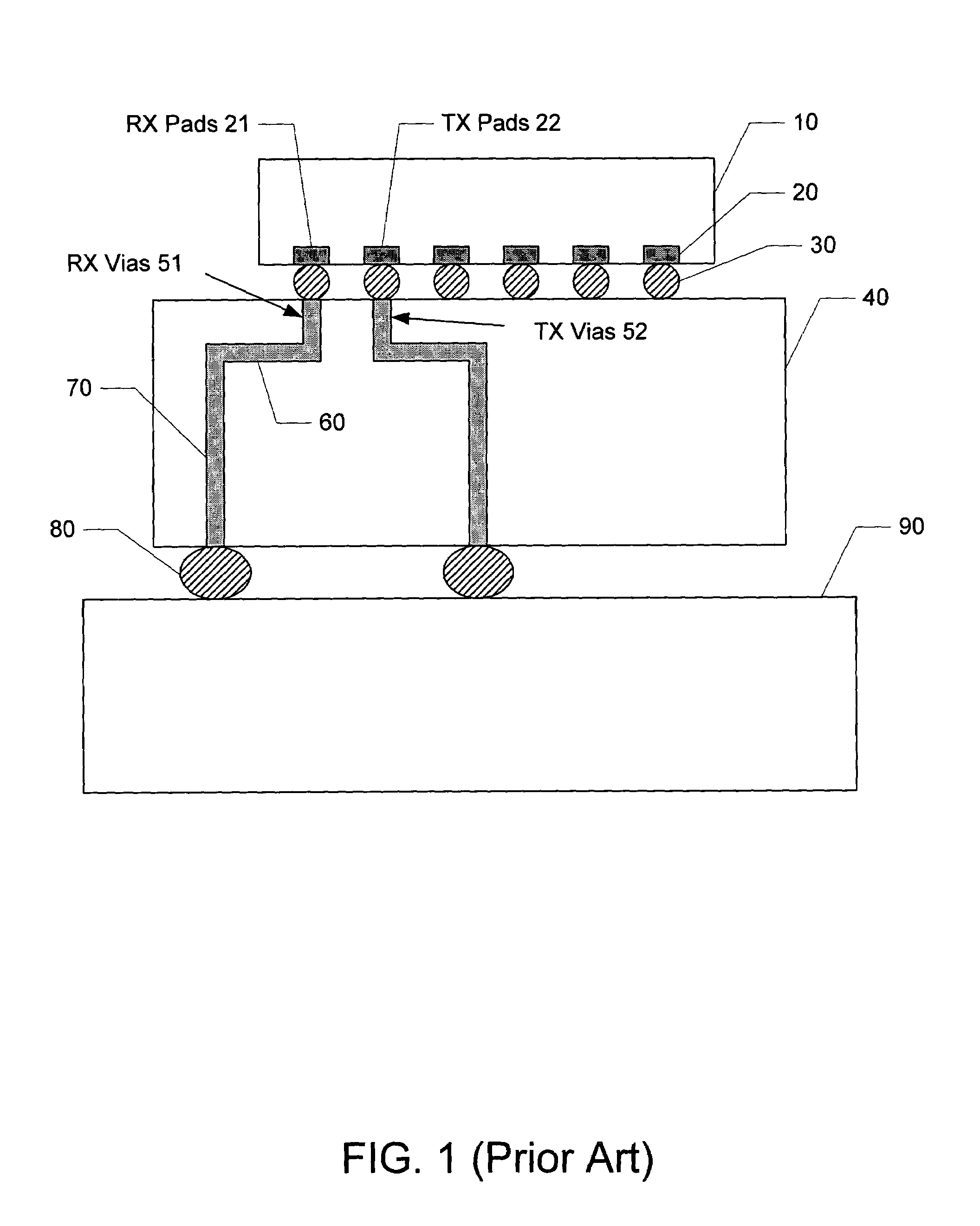
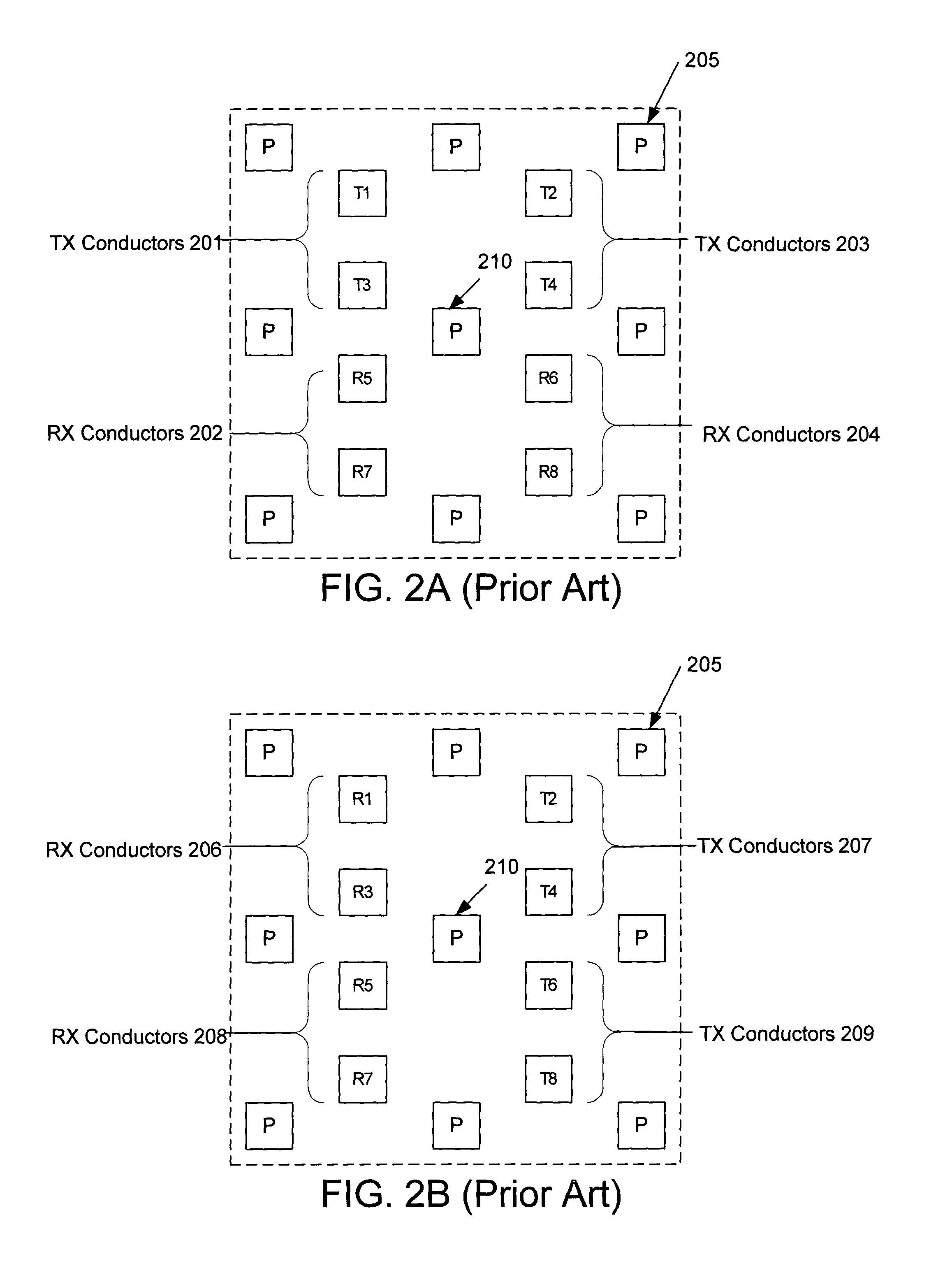
FIELD OF THE INVENTION[0001]The present invention relates to semiconductor chips, and more particularly to semiconductor chip packages.BACKGROUND OF THE INVENTION[0002]As the number of integrated circuits in electronic systems increases, and the size of the individual devices decreases, the density of interconnections, as well as the number of input / outputs (I / Os), are progressively increased year after year. Accordingly, semiconductor chip package technology are also improved in areas such as capacity, quality and cost. For a package with high-density interconnects and I / Os, cross-talk related signal integrity is a concern. To illustrates this problem, please refer to FIGS. 1, 2A, and 2B.[0003]FIG. 1 illustrates a cross-sectional view of a conventional thin-film chip package. The package comprises a semiconductor chip 10 having a plurality of pads 20 and Controlled Collapse Chip Connection (C4) balls 30. The chip 10 is flipped such that the C4 balls 30 are bounded to a carrier 40. ...

Claims


Application Information

Patent Timeline
Patent Type & Authority Patents(United States)
IPC IPC(8): H01L23/48H01L23/12H01L23/64
CPCH01L23/642H01L2924/15174H01L2224/16225H01L2924/3025H01L2924/15311H01L2224/05571H01L2224/05573H01L2924/00014H01L2224/05599
Inventor BUFFET, PATRICK H.CHIU, CHARLES S.GARLETT, JON D.HSU, LOUIS L.SCHUH, BRIAN J.
Owner INT BUSINESS MASCH CORP
Why Eureka
Try Eureka