

AGC circuit
a gain control and circuit technology, applied in amplifiers, amplifiers with semiconductor devices/discharge tubes, amplifiers, etc., can solve the problem that the capacitance value of the integrator circuit is too large to be and achieve the effect of being easily incorporated in an integrated circui
- Summary
- Abstract
- Description
- Claims
- Application Information
AI Technical Summary
Benefits of technology
Problems solved by technology
Method used
Image

Examples
embodiment 1
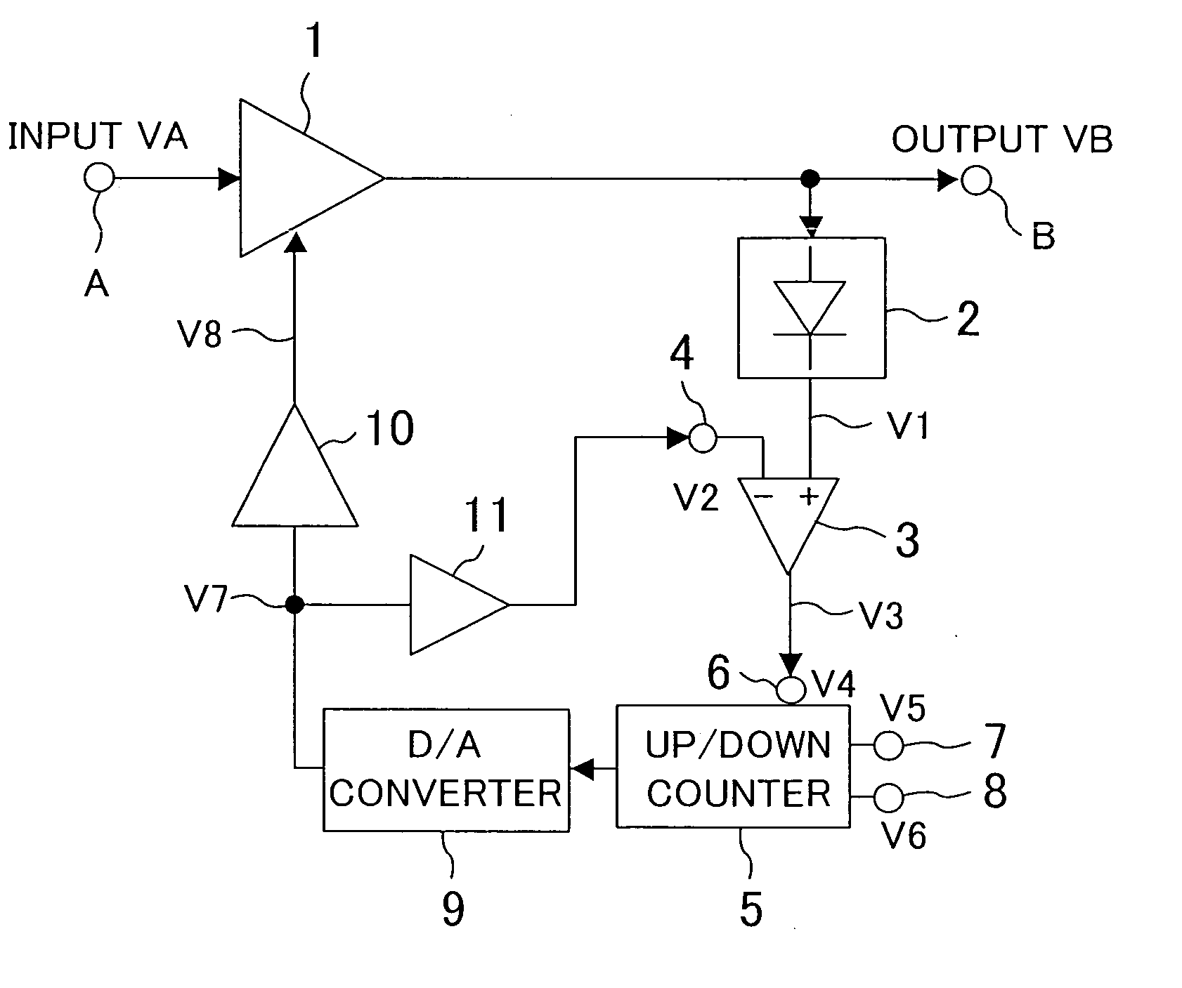
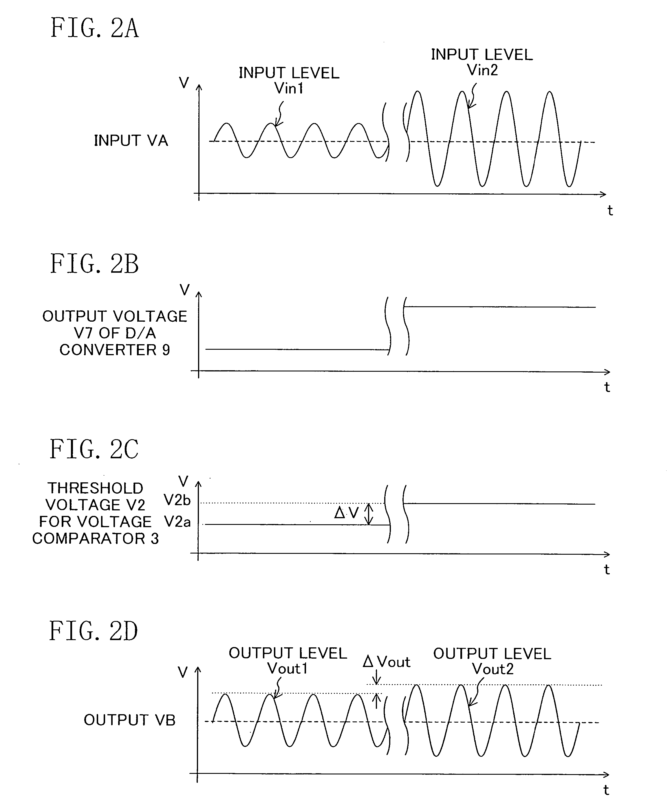
[0023]FIG. 1 shows a configuration of an AGC circuit of Embodiment 1 of the present invention. Referring to FIG. 1, the AGC circuit includes a variable gain amplifier circuit 1, a rectifier circuit 2, a voltage comparator 3, an up / down counter 5, a D / A converter circuit 9, a first DC amplifier circuit 10 and a second DC amplifier circuit 11. The variable gain amplifier circuit 1 amplifies or attenuates an input signal VA received via a signal input terminal A according to the gain controlled with a gain control voltage V8 and outputs an output signal VB via an output terminal B. The rectifier circuit 2 rectifies the output voltage of the variable gain amplifier circuit 1. Hereinafter, the rectifier circuit 2 will be described as being a full-wave rectifier circuit. Alternatively, the rectifier circuit 2 may be a half-wave rectifier circuit. The voltage comparator circuit 3 compares a rectified signal (output signal) V1 of the rectifier circuit 2 with a threshold voltage V2, and outp...
embodiment 2
[0035]FIG. 6 shows a configuration of an AGC circuit of Embodiment 2 of the present invention. In FIG. 6, the same components as those of the AGC circuit of FIG. 1 are denoted by the same reference numerals, and description thereof is omitted here. Only the components newly added to the AGC circuit of FIG. 1 will be described hereinafter. Note that in this embodiment, the voltage comparator 3, the up / down counter 5 and the D / A converter circuit 9 described above are respectively called the “first voltage comparator”, the “first up / down counter” and the “first D / A converter circuit”. Referring to FIG. 6, the AGC circuit further includes a second up / down counter 14, a second D / A converter circuit 18, a second voltage comparator 19 and a switch circuit 20. The second up / down counter 14 has an up / down counting control input terminal 15 for receiving a control signal V10 for control of the direction of counting of the second up / down counter 14, an input terminal 16 for a clock V11 for up...
embodiment 3
[0050]FIG. 8 shows a configuration of an AGC circuit of Embodiment 3 of the present invention. In FIG. 8, a clock switch circuit 21 is provided in place of the switch circuit 20 in FIG. 6. In FIG. 8, the same components as those of the AGC circuit of FIG. 6 are denoted by the same reference numerals, and description thereof is omitted here. Only the component newly added to the AGC circuit of FIG. 6 will be described hereinafter. The clock switch circuit 21 in FIG. 8 receives the output voltage V14 of the second voltage comparator 19 and switches the frequency of the count clock V5 or V6 for the first up / down counter 5 according to the level of the voltage V14 received via a clock switch control input terminal 22.
[0051] The AGC circuit of FIG. 6 described above has the following problem. When the input offset of the second voltage comparator 19 is large, the difference between the output voltage V7 of the first D / A converter circuit 9 and the output voltage V13 of the second D / A con...
PUM
 Abstract
Description
Claims
Application Information