Wafer level creation of multiple optical elements

Inactive Publication Date: 2005-01-18
AVAGO TECH WIRELESS IP SINGAPORE PTE
View PDF11 Cites 142 Cited by
  • Summary
  • Abstract
  • Description
  • Claims
  • Application Information

AI Technical Summary

Benefits of technology

Considering the foregoing background, it is an object of the present invention to efficiently produce integrated multiple opt

Problems solved by technology

Alignment accuracies of less than 15 microns for individual elements can be achieved using active alignment, but such accuracies greatly increase the amount of time spent moving the element.
Thus, such alignment accuracy is often impractical even using active alignment.
The alignment tolerance needed may be 1 micron to 5 microns, which is very expensive to achieve with conventional methods.
However, passive alignment has not been employed for wafer-to-wafer alignment.
In particular, the high density of solder bumps required and the thickness and mass of the wafer make such alignment impractical.
Another problem in integrating multiple optical elements formed on separate wafers at a wafer level arises due to the dicing process for forming the individual integrated elements.
The dicing process is messy due to the use of a dicing slurry.
However, when the wafers are bonded together, the slurry enters the gap between the wafers.
Removing the slurry from the gap formed between the wafers is quite difficult.
Glass molding however has disadvantages of being expensive to make tooling and limited in siz

Method used


Image

  • Wafer level creation of multiple optical elements
  • Wafer level creation of multiple optical elements
  • Wafer level creation of multiple optical elements

Examples


Example

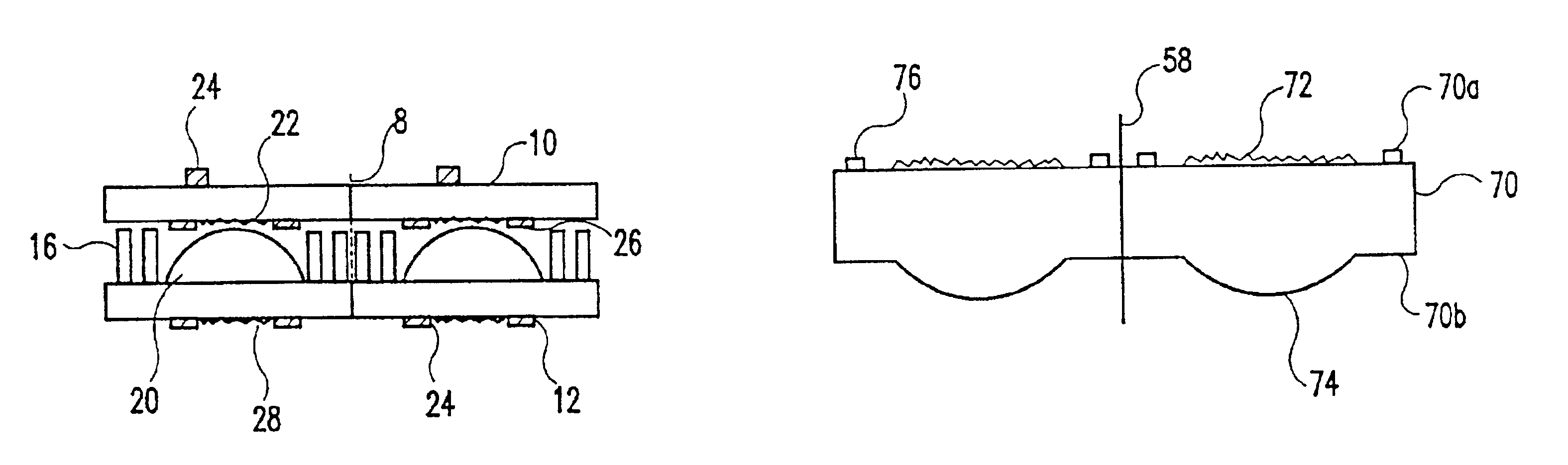
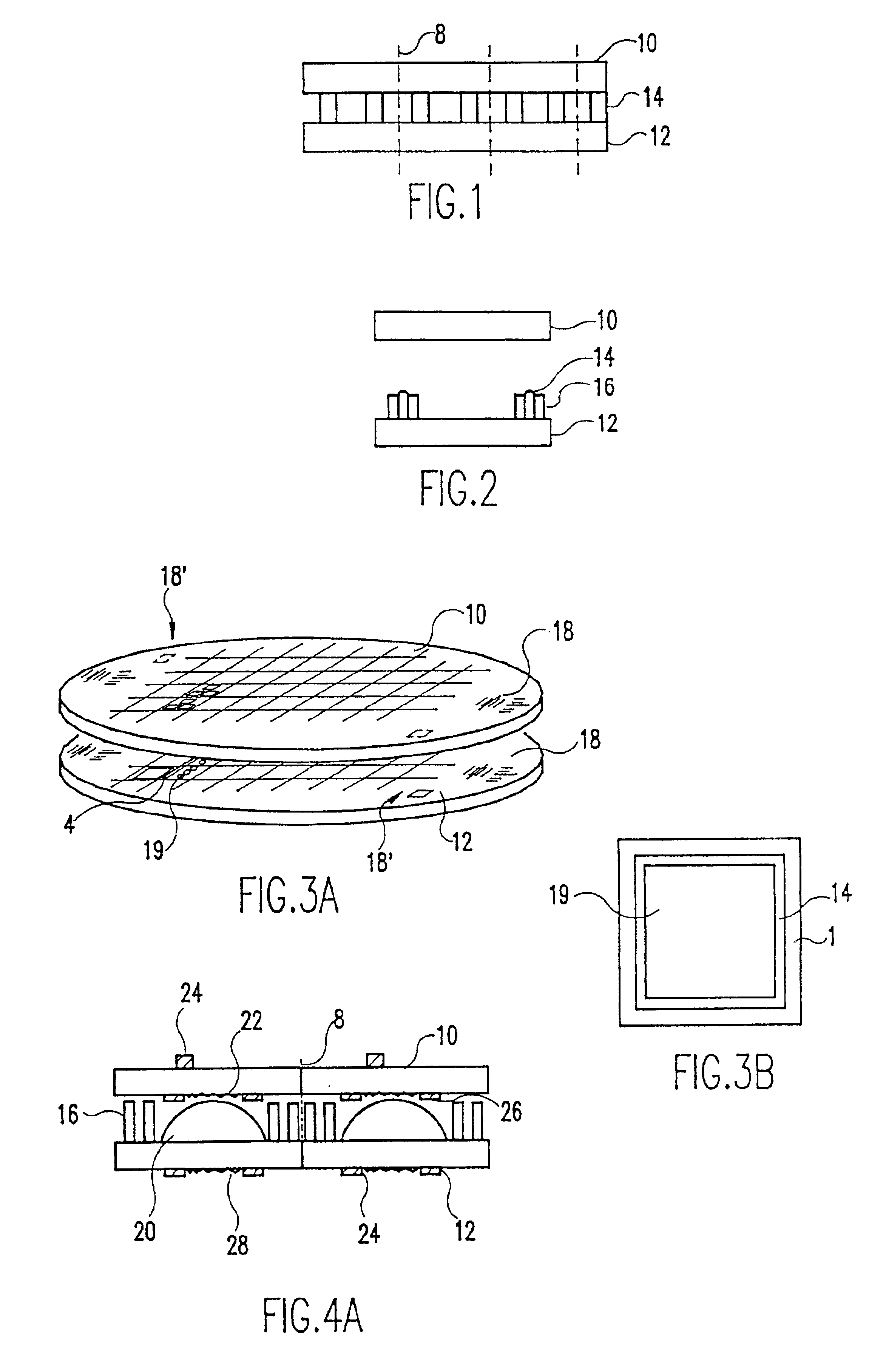
As can be seen in FIG. 1, a first substrate wafer 10 and a second substrate wafer 12 are to be bonded together in order to provide integrated multiple optical elements. A wafer is a disc, typically 4, 6, 8, or 12 inches in diameter and typically having a thickness between 400 microns and 6 mm.

These wafers have an array of respective optical elements formed thereon on either one or both surfaces thereof. The individual optical elements may be either diffractive, refractive or a hybrid thereof. Dashed lines 8 indicate where the dicing is to occur on the wafers to provide the individual integrated elements.

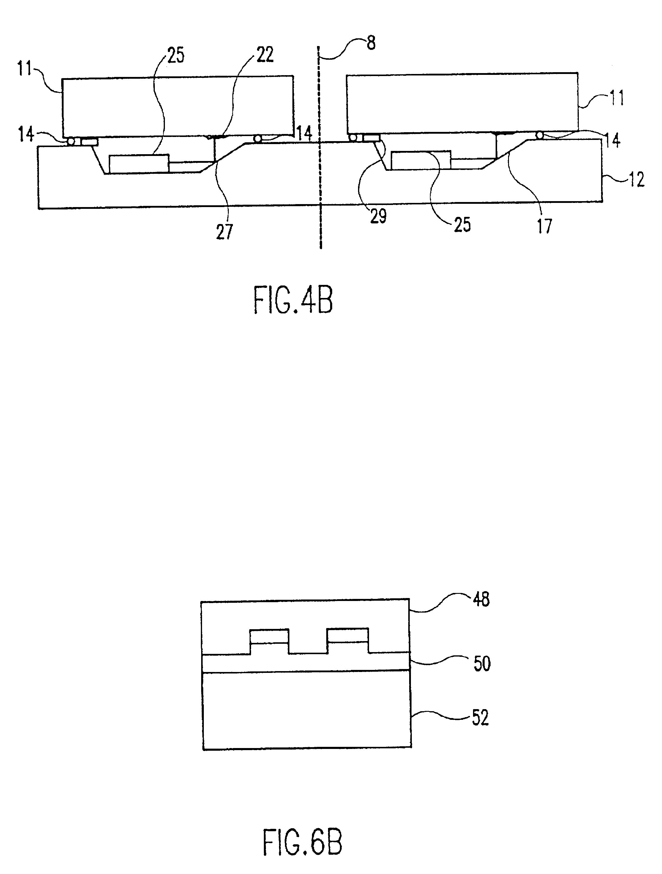
A bonding material 14 is placed at strategic locations on either substrate in order to facilitate the attachment thereof. By surrounding the optical elements which are to form the final integrated die, the adhesive 14 forms a seal between the wafers at these critical junctions. During dicing, the seal prevents dicing slurry from entering between the elements, which would result in co...


PUM

PropertyMeasurementUnit
Poweraaaaaaaaaa
Areaaaaaaaaaaa
Opacityaaaaaaaaaa

Abstract

Integrated multiple optical elements may be formed by bonding substrates containing such optical elements together or by providing optical elements on either side of the wafer substrate. The wafer is subsequently diced to obtain the individual units themselves. The optical elements may be formed lithographically, directly, or using a lithographically generated master to emboss the elements. Alignment features facilitate the efficient production of such integrated multiple optical elements, as well as post creation processing thereof on the wafer level.

Description

FIELD OF THE INVENTIONThe present invention is directed to integrating multiple optical elements on a wafer level. In particular, the present invention is directed to efficient creation of integrated multiple elements.BACKGROUND OF THE INVENTIONAs the demand for smaller optical components to be used in a wider variety of applications increases, the ability to efficiently produce such optical elements also increases. In forming such integrated multiple optical elements at a mass production level, the need for accurate alignment increases. Further, such alignment is critical when integrating more than one optical element.Integrated multiple optical elements are multiple optical elements stacked together along the z-axis, i.e., the direction of the light propagation. Thus, light travelling along the z-axis passes through the multiple elements sequentially. These elements are integrated such that further alignment of the elements with themselves is not needed, leaving only the integrate...

Claims


Application Information

Patent Timeline
IPC IPC(8): H01L25/16G02B6/12G02B6/42G03F9/00G11B7/12G11B7/135G11B7/22H01L27/00H01L27/146H01L31/12H01S3/00H01S5/00H01S5/022
CPCG02B6/4206G02B6/4231G02B6/4232G03F9/7042G11B7/1205G11B7/1353G11B7/1362G11B7/1372G11B7/22H01L25/167H01L27/14625H01L27/14632H01L27/14687G02B5/1819G02B13/0085G02B3/0006Y10T156/1052G02B6/4224G02B6/4238G02B6/4239G02B2006/12102G02B2006/12107G11B2007/13727H01S5/0201H01S5/02248Y10T156/1092Y10T156/1089G02B6/4214H01L2924/0002G11B7/123H01S5/02325H01L2924/00H01L25/16
Inventor HARDEN, BRIANKATHMAN, ALANFELDMAN, MICHAEL
Owner AVAGO TECH WIRELESS IP SINGAPORE PTE
Why Eureka
Try Eureka