Elastic micro probe and method of making same

a micro-probe and elastic technology, applied in the field of elastic micro-probes, can solve the problems of low stability, unusable wear and tip contact instability, and complicated assembly of precision parts, and achieve the effects of saving manufacturing time, reducing labor-intensive assembly procedures, and improving product precision

Inactive Publication Date: 2006-09-21
MICROELECTRONICS TECH INC
View PDF3 Cites 27 Cited by
  • Summary
  • Abstract
  • Description
  • Claims
  • Application Information

AI Technical Summary

Benefits of technology

[0009] It is another object of the present invention to provide an elastic micro probe manufacturing process, which employs micro electromechanical technology to reduce labor-intensive assembly procedure, thereby saving much manufacturing time and improving product precision.
[0010] It is still another object of the present invention to provide an elastic micro probe manufacturing process, which is practical for the fabrication of elastic micro probes that have the solder joint disposed at the top side so as to facilitate the maintenance and replacement of probes.
[0011] It is still another object of the present invention to provide an elastic micro probe manufacturing process, which is practical for the fabrication of micro spring contacts that have the solder joint and the tip set close to each other for positive positioning to achieve a high precision.
[0012] It is still another object of the present invention to provide an elastic micro probe manufacturing process, which employs an embedded architecture, preventing damage of the spring by an external force.
[0013] According to the present invention, the elastic micro probe comprises an electrically conductive and stretchable spring, which has a first end, a second end opposite to the first end, and at least one connection point disposed adjacent to the first end for connection to an external circuit; an electrically conductive probe body, which has a first end connected to the second end of the spring and a second end vertically upwardly protruding over the first end of the spring; and an electrically conductive tip, which has a bottom side connected to the second end of the probe body such that when the tip is pressed, the probe body is forced to move the second end of the spring, thereby causing the spring to be stretched and elastically deformed.

Problems solved by technology

However, it is complicated to assemble the precision parts.
Because the spring member for this elastic probe is a thin and elongated metal wire member, it has a low stability.
When compressed, the spring member may be biased to rub against the peripheral wall, resulting in unnecessary wearing and tip contact instability.
Following the development of miniaturized semiconductor and package technology, this design of spring probe cannot meet actual requirements.
Further, the alignment error of the multilayer structure between the solder joint 2 and the tip 4 cannot assure accurate positioning of the tip during bonding.
Further, because the spring probe is completely exposed to the outside, it tends to be damaged.

Method used


Image

  • Elastic micro probe and method of making same
  • Elastic micro probe and method of making same
  • Elastic micro probe and method of making same

Examples


first embodiment

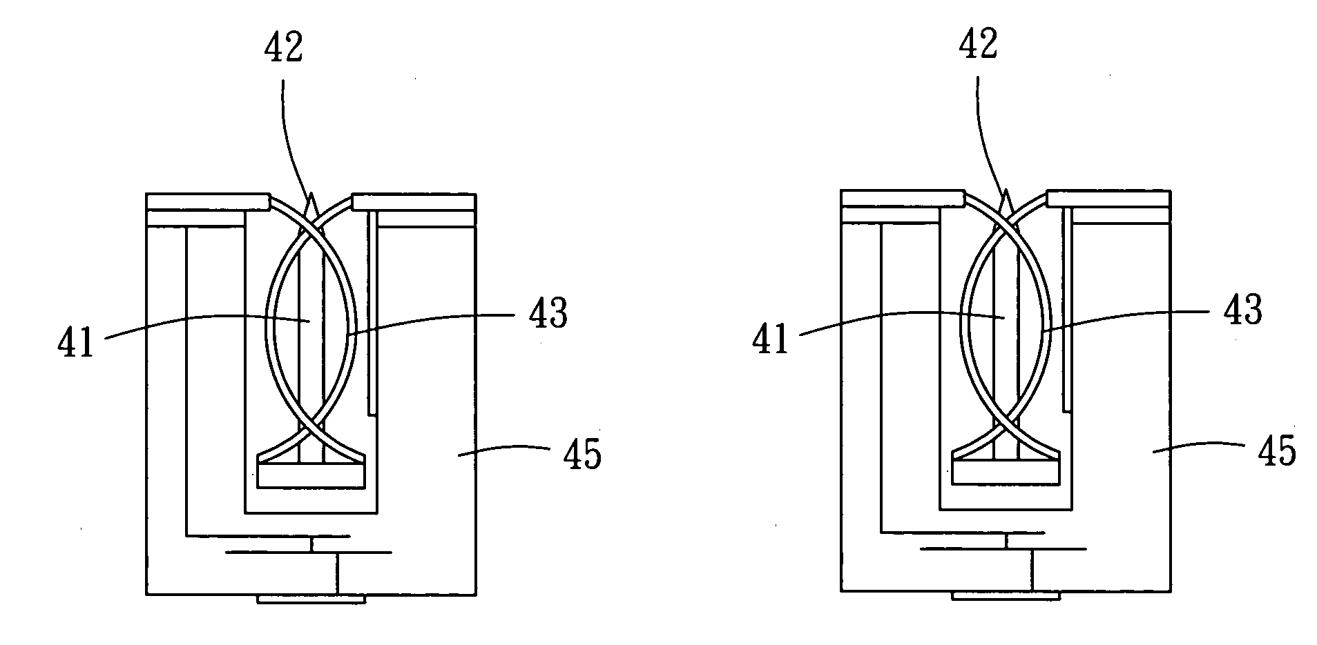
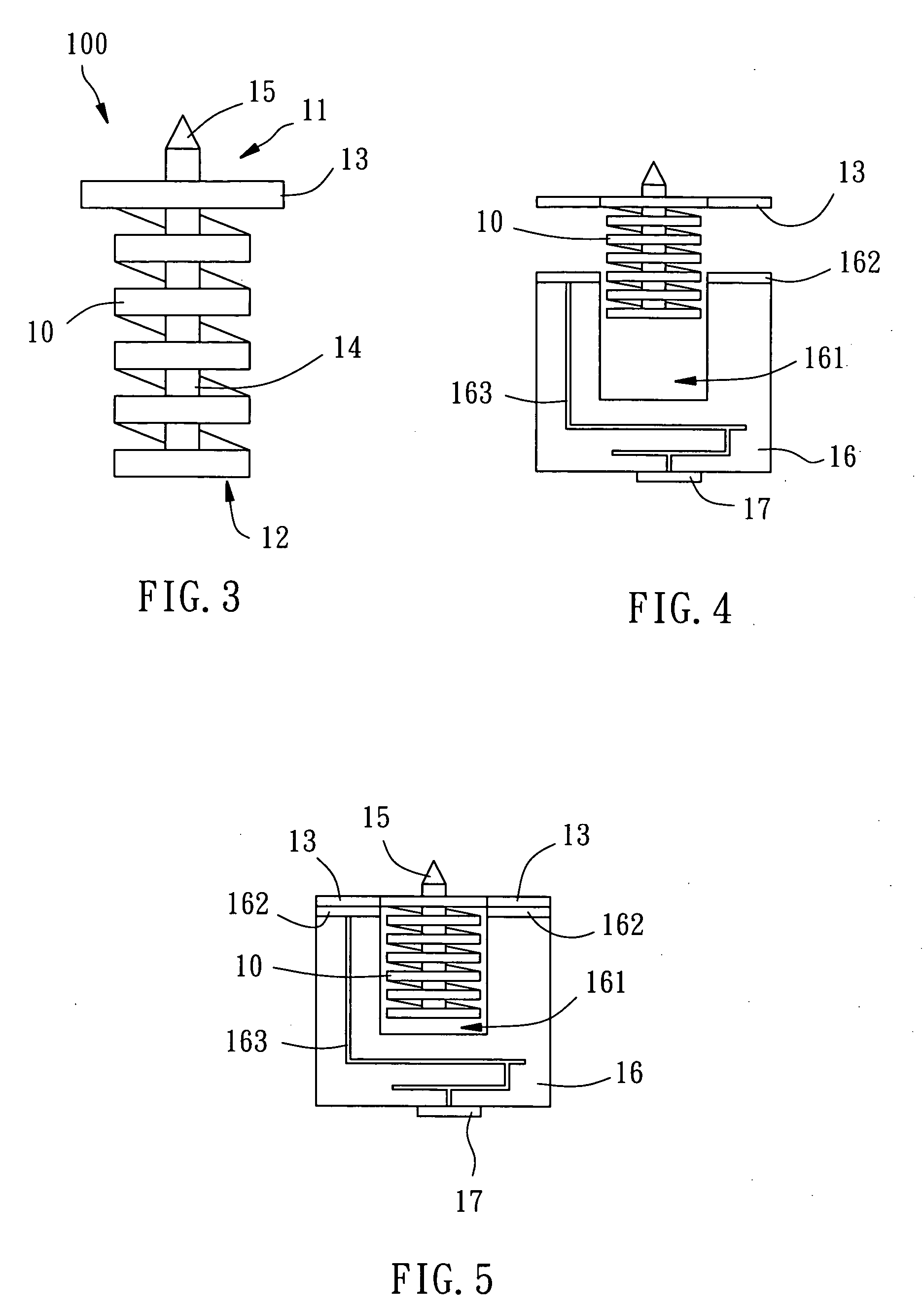
[0039] Referring to FIG. 3, an elastic micro probe 100 in accordance with the present invention is shown comprising a spring 10, a probe body 14, and a tip 15.

[0040] The spring 10 is an electrically conductive, single-screw, compressible, stretchable, hollow member made through micro electromechanical technology, having a first end 11, a second end 12 opposite to the first end 11, and two connection points 13 disposed adjacent to the first end 11 at two sides.

[0041] The probe body 14 is an electrically conductive, rod-like member set inside the spring 10, having one end, namely, the bottom end connected to the second end 12 of the spring 10 and the other end, namely, the top end vertically upwardly protruding over the first end 11 of the spring 10.

[0042] The tip 15 is an electrically conductive, conical member or pyramid, having the bottom side thereof connected to the free end (top end) of the probe body 14.

[0043]FIGS. 4-6 show the assembly process of the elastic micro probe 100...

second embodiment

[0045]FIGS. 8a-8h show an elastic micro probe manufacturing method according to the present invention. According to this manufacturing method, a socket and an elastic micro probe are made in integrity, thereby simplifying the manufacturing process. This manufacturing method includes the steps of:

[0046] (a) preparing a substrate 70 having a circuit 71 as shown in FIG. 8a;

[0047] (b) laying a shielding layer 72 having a patterned opening on the circuit 71 of the substrate 70 as shown in FIG. 8b, which shielding layer 72 can be photoresist and which patterned opening can be achieved by means of a semiconductor photo lithographic technology;

[0048] (c) depositing a conductive layer 73 on the top side of the substrate 70 and the shielding layer 72 by evaporation deposition, sputtering deposition, or electroplating as shown in FIG. 8c;

[0049] (d) forming a sacrificial layer 74 on the top side of the conductive layer 73 and leveling the sacrificial layer 74 by grinding as shown in FIG. 9d,...

fourth embodiment

[0067]FIGS. 10a-10j show an elastic micro probe manufacturing method according to the present invention. The above-mentioned embodiment is to make an elastic micro probe directly on a substrate by lamination. Alternatively, the socket and the probe body can be produced at the same time and then fastened to the substrate. The manufacturing method according to this embodiment comprises the steps of:

[0068] (A) preparing a substrate 90 having a conical notch 91 at the top side thereof (the conical notch of the substrate can be made by a precision machine processing process, chemical etching, or hot press molding) and then depositing a conductive material 92 on the top surface of the substrate 90 as shown in FIG. 10a (the conductive material can be deposited on the substrate by evaporation deposition, sputtering deposition, or electroplating);

[0069] (B) depositing an enhanced film 93 on the surface of the notch 91 subject to the use of a mask (similar to FIG. 9k) by means of sputtering ...


PUM


Abstract

An elastic micro probe includes an electrically conductive and stretchable spring, which has a first end, a second end opposite to the first end, and connection points disposed adjacent to the first end for connection to an external element, an electrically conductive probe body, which has a first end connected to the second end of the spring and a second end vertically upwardly protruding over the first end of the spring, and an electrically conductive tip, which has a bottom side connected to the second end of the probe body such that when the tip is pressed, the probe body is forced to move the second end of the spring, thereby causing the spring to be stretched and elastically deformed.

Description

BACKGROUND OF THE INVENTION [0001] 1. Field of the Invention [0002] The present invention relates to micro probes and more particularly, to an elastic micro probe for use as a circuit connection interface. The invention relates also to the fabrication of the elastic micro probe. [0003] 2. Description of the Related Art [0004] When testing high-density or high-speed electrical devices (for example, LSI or VLSI circuits), a probe card having a big amount of elastic micro contacts (probes) shall be used. By means of the resilient and electrically conductive material property of the elastic micro probes, the probe card is used as an electric connection medium between the test apparatus and the device to be tested, for example, an LSI chip, VLSI chip, semiconductor wafer, semiconductor chip, semiconductor package, or printed circuit board. Elastic micro contacts can also be used as lead wire means for an IC package. For easy understanding of the present invention, elastic micro contacts ...

Claims


Application Information

Patent Timeline
Patent Type & Authority Applications(United States)
IPC IPC(8): G01R31/02
CPCG01R3/00G01R1/06733G01R1/06722
Inventor CHEN, CHIH-CHUNG
Owner MICROELECTRONICS TECH INC
Why Eureka
Try Eureka