

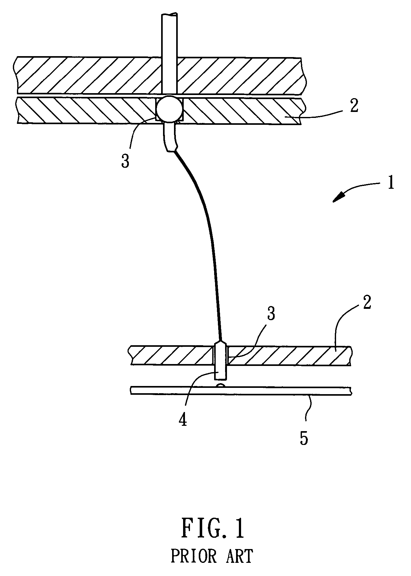
Method for making guide panel for vertical probe card in batch
a technology of vertical probe and guide panel, which is applied in the direction of electrical measurement instrument details, measurement devices, instruments, etc., can solve the problems of not meeting the requirements of modem technology, the method is relatively expensive, and the position precision of micro feed through holes is limited, so as to save manufacturing time and reduce manufacturing costs.
- Summary
- Abstract
- Description
- Claims
- Application Information
AI Technical Summary
Benefits of technology
Problems solved by technology
Method used
Image

Examples
first embodiment
[0040] Similar to the aforesaid first embodiment, the guide panel thus obtained can be cut into small guide panels, i.e. the method further includes the following steps.
[0041] (G) As shown in FIG. 3G; the guide panel 20 thus obtained from step (F) is cut into small guide panels 20.
[0042] (H) The guide panel 20 thus obtained is bonded to a seat member 23, as shown in FIG. 3H.
[0043] Further, an insulative material, such as SiO2, Al2O3, TiO2, or any suitable dielectric material may be coated on the guide panel to enhance the insulative characteristic.
[0044] Further, a polymeric material, such as polyimide, may be coated on the guide panel to enhance the toughness of the guide panel or the lubricant characteristic of the micro feed through holes.
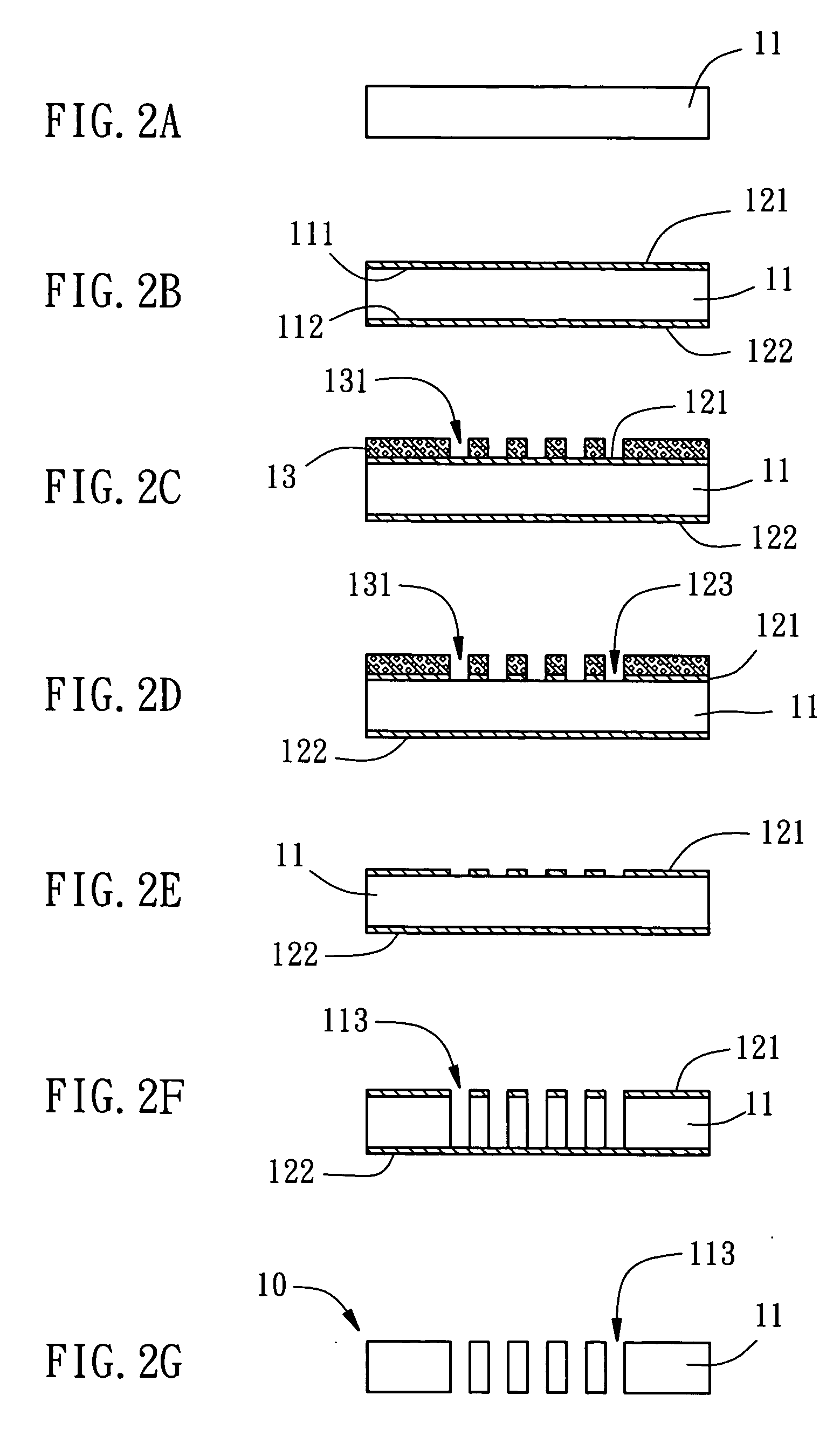
[0045]FIGS. 4A-4I show a guide panel fabrication method according to a third preferred embodiment of the present invention. According to this embodiment, the guide panel fabrication method includes the following steps.
[0046] (A) As shown in...
fifth embodiment
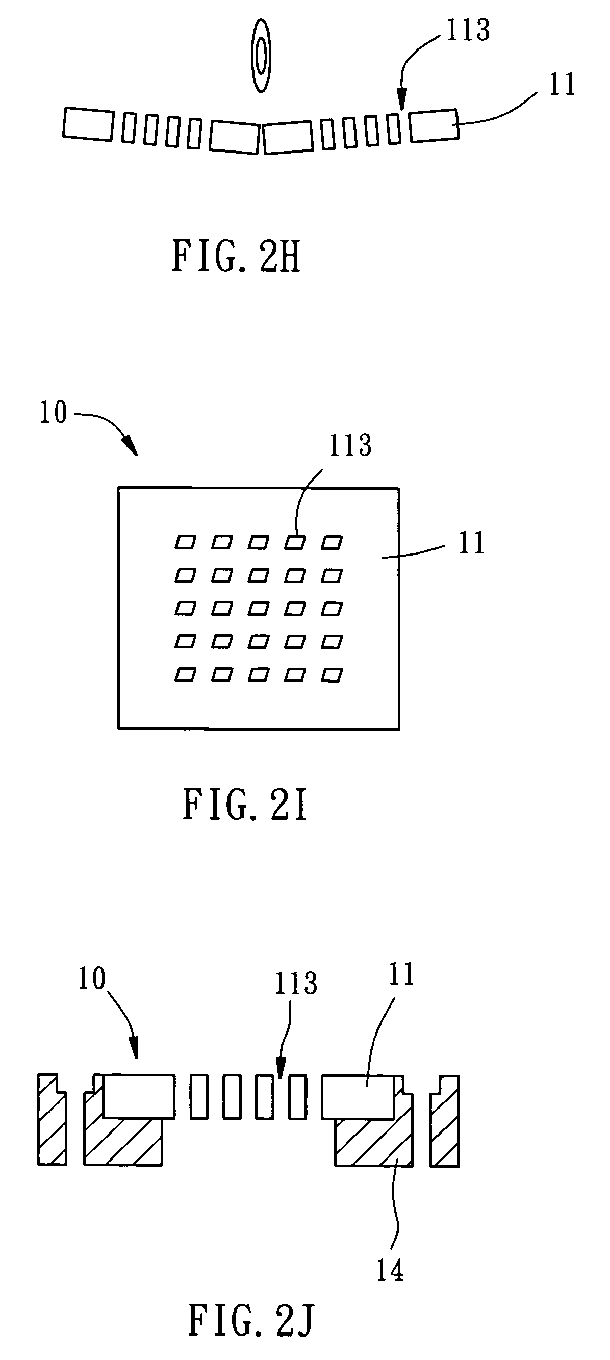
[0082] (J) As shown in FIG. 6J, the first oxide layer 521 and the second oxide layer 522 are removed, thereby obtaining the desired guide panel 50. As shown in FIG. 6J, the guide panel 50 has a bottom portion acting as the seat member 14 of FIG. 2J. In other words, by means of this method of the fifth embodiment the substrate 11 and the seat member 14 of FIG. 2J can be integrally formed.
[0083]FIG. 6K is a top view of FIG. 6J. As shown in FIG. 6K, the two relatively greater through holes at two opposite lateral sides of the guide panel 50 are providing for mounting on an external object.
[0084] According to the aforesaid five embodiments, the present invention provides a guide panel fabrication method, which uses the anisotropic etching technique to make micro feed through holes on a substrate so that the guide panels for vertical probe card can be made in batch at a time to save the manufacturing time and to reduce the manufacturing cost. Further, the method of the present invention...
PUM
| Property | Measurement | Unit |
|---|---|---|
| semiconductor | aaaaa | aaaaa |
| anisotropic | aaaaa | aaaaa |
| polymeric | aaaaa | aaaaa |
Abstract
Description
Claims
Application Information