This helps you quickly interpret patents by identifying the three key elements:
Problems solved by technology
Method used
Benefits of technology
Benefits of technology
[0012] An object of the present invention is to provide a semiconductor device capable of providing higher performance of a package, enhancing heat dissipation and high-frequency characteristics, reducing the influence of the noise, and enabling easy lamination.
Problems solved by technology
However, in the semiconductor device disclosed in Patent Publication 1 having laminated semiconductor chips, the heat generated by the respective semiconductor chips is not well dissipated, and therefore the heat may adversely affects the operation of the semiconductor chips or the like.
Further, in the semiconductor devices disclosed in Patent Publications 2, 3 and 4, the semiconductor chips are surrounded by the base frame (Patent Publication 2) or the extension portion (Patent Publications 3 and 4) made of, for example, resin or organic material, and therefore the heat dissipation of the semiconductor chips may be reduced, so that the high-frequency characteristics may be adversely affected.
Method used
Image
Click on the blue label to locate the original text in one second.
Reading with bidirectional positioning of images and text.
Examples
first embodiment
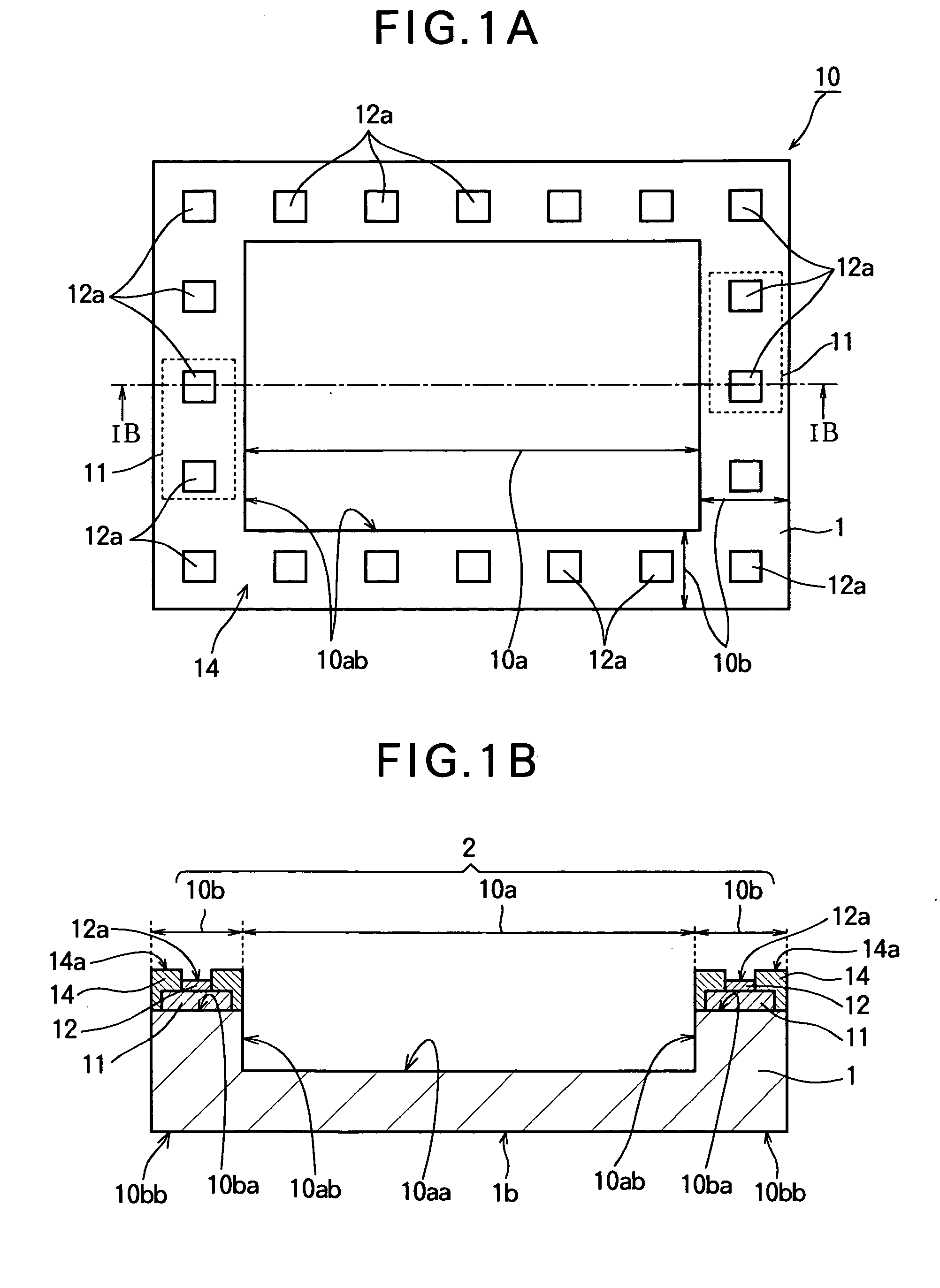
[0065] The first embodiment of the present invention will be described with reference to FIGS. 1A and 1B. The first embodiment relates to a frame-shaped semiconductor chip.
[0066]FIG. 1A is a schematic plan view of a frame-shaped semiconductor chip according to the first embodiment, as seen from above. FIG. 1B is a schematic sectional view taken along line IB-IB in FIG. 1A.
[0067] As shown in FIGS. 1A and 1B, the frame-shaped semiconductor chip 10 is formed on a semiconductor substrate 1 such as a siliconwafer.
[0068] The frame-shaped semiconductor chip 10 includes the semiconductor substrate 1 having an opening portion 10a and a frame portion 10b that constitutes a periphery around the opening portion 10a.
[0069] The frame-shaped semiconductor chip 10 is in the shape of, for example, a square. The frame portion 10b has a top surface 10ba and a bottom surface 10bb. The bottom surface 10bb is aligned with a bottom surface 1b of the s...
second embodiment
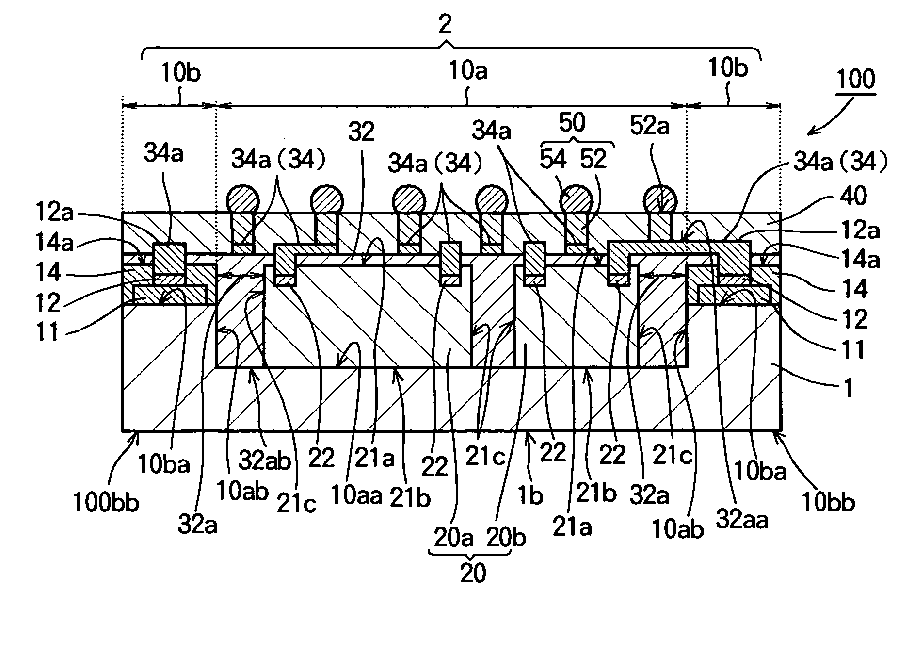
[0099] The second embodiment of the present invention will be described with reference to FIGS. 4A through FIGS. 7C. The second embodiment relates to a semiconductor device using the above described frame-shaped semiconductor chip 10, i.e., a semiconductor device of the SIP structure.
[0100]FIG. 4A is a schematic plan view illustrating the semiconductor device of the SIP structure. In FIG. 4A, a sealing portion is omitted, in order to clearly show the positional relationship between the electrode pads and the wiring layer. FIG. 4B is a schematic sectional view taken along Line IVB-IVB in FIG. 4A.
[0101] As shown in FIGS. 4A and 4B, the semiconductor device 100 of the SIP structure of this embodiment includes the frame-shaped semiconductor chip having above described structure.
[0102] At least one mountable semiconductor chip (i.e., second semiconductor chip) 20 is mounted in the opening portion 10a of the frame-shaped semiconductor chip 1...
third embodiment
[0169] The third embodiment of the present invention will be described with reference to FIG. 8. The third embodiment is different from the second embodiment in structure of the semiconductor device (SIP). In the third embodiment, a lower base having functionality is formed on the lower side of the package.
[0170] In the third embodiment, the components formed on the upper side of the semiconductor substrate 1 (i.e., the electric devices 11, the wiring layer 34, the insulation films 14 and 32, the sealing portion 40 and the external terminals 50) are the same as those of the second embodiment. Therefore, the components that are the same as those of the second embodiment are assigned the same reference numerals, and the explanation thereof is omitted.
[0171]FIG. 8 is a schematic sectional view of the semiconductor device cut along a line corresponding to Line IVB-IVB in FIG. 4A.
[0172] In this example, the semiconductor device 100 has a lower base 60 formed on the bottom side thereof...
PUM
Abstract
A semiconductorchip includes a semiconductor substrate having an opening portion and a frame portion defining a periphery of the opening portion. At least one electric element is provided on the frame portion, and has at least one electrode terminal. A first insulation film is formed on the frame portion so that the electrode terminal is partially exposed at the first insulation film to form a plurality of electrode pads.
Description
BACKGROUND OF THE INVENTION [0001] This invention relates to a semiconductor device having System-In-Package (SIP) structure. [0002] The semiconductor device of the SIP structure is formed by sealing a plurality of semiconductor chips in a single package to form an integrated system. The semiconductor device of the SIP structure has advantages of low electric power consumption, high performance, and small mounting area. [0003] Particularly, there is known a semiconductor device called as Wafer-Level SIP, which is formed by sealing the semiconductor chips on a wafer and separating the wafer into individual semiconductor devices. [0004] For example, there is known a semiconductor device of the SIP structure in which a second semiconductor chip is laminated on a first semiconductor chip, and a protection film (thicker than the second semiconductor chip) is formed on the first semiconductor chip. The protection film has a hole (having the same size as the second semiconductor chip) in w...
Claims
Application Information
Patent Timeline
Application Date:The date an application was filed.
Publication Date:The date a patent or application was officially published.
First Publication Date:The earliest publication date of a patent with the same application number.
Issue Date:Publication date of the patent grant document.
PCT Entry Date:The Entry date of PCT National Phase.
Estimated Expiry Date:The statutory expiry date of a patent right according to the Patent Law, and it is the longest term of protection that the patent right can achieve without the termination of the patent right due to other reasons(Term extension factor has been taken into account ).
Invalid Date:Actual expiry date is based on effective date or publication date of legal transaction data of invalid patent.

