Method and apparatus employing dynamic element matching for reduction of column-wise fixed pattern noise in a solid state imaging sensor

a dynamic element matching and solid-state imaging technology, applied in the field of semi-conductor imaging devices, can solve the problems of not easy or cheap to test the capacitance value, and achieve the effect of reducing the visual obviousness of column-wise fixed pattern nois

Inactive Publication Date: 2006-10-19
APTINA IMAGING CORP
View PDF10 Cites 50 Cited by
  • Summary
  • Abstract
  • Description
  • Claims
  • Application Information

AI Technical Summary

Benefits of technology

[0010] An imager is provided in an exemplary embodiment that reduces the visual obviousness of column-wise fixed pattern noise by randomly mixing and applying fixed pattern noise to different columns in the imager's array. In an exemplary embodiment of the invention, signals from the columns of the pixel array are read out to varying sample and hold circuits selected at random. In addition, pixel columns are randomly matched to sample and hold circuits.

Problems solved by technology

However, it is not easy or cheap to test the capacitance value of each capacitor c_rst, c_sig and then modify the capacitors to have the same capacitance value.

Method used


Image

  • Method and apparatus employing dynamic element matching for reduction of column-wise fixed pattern noise in a solid state imaging sensor
  • Method and apparatus employing dynamic element matching for reduction of column-wise fixed pattern noise in a solid state imaging sensor
  • Method and apparatus employing dynamic element matching for reduction of column-wise fixed pattern noise in a solid state imaging sensor

Examples


Embodiment Construction

[0016] In the following detailed description, reference is made to the accompanying drawings, which form a part hereof, and in which is shown by way of illustration specific exemplary embodiments of the invention. These embodiments are described in sufficient detail to enable those of ordinary skill in the art to make and use the invention, and it is to be understood that structural, logical or other changes may be made to the specific embodiments disclosed without departing from the spirit and scope of the present invention.

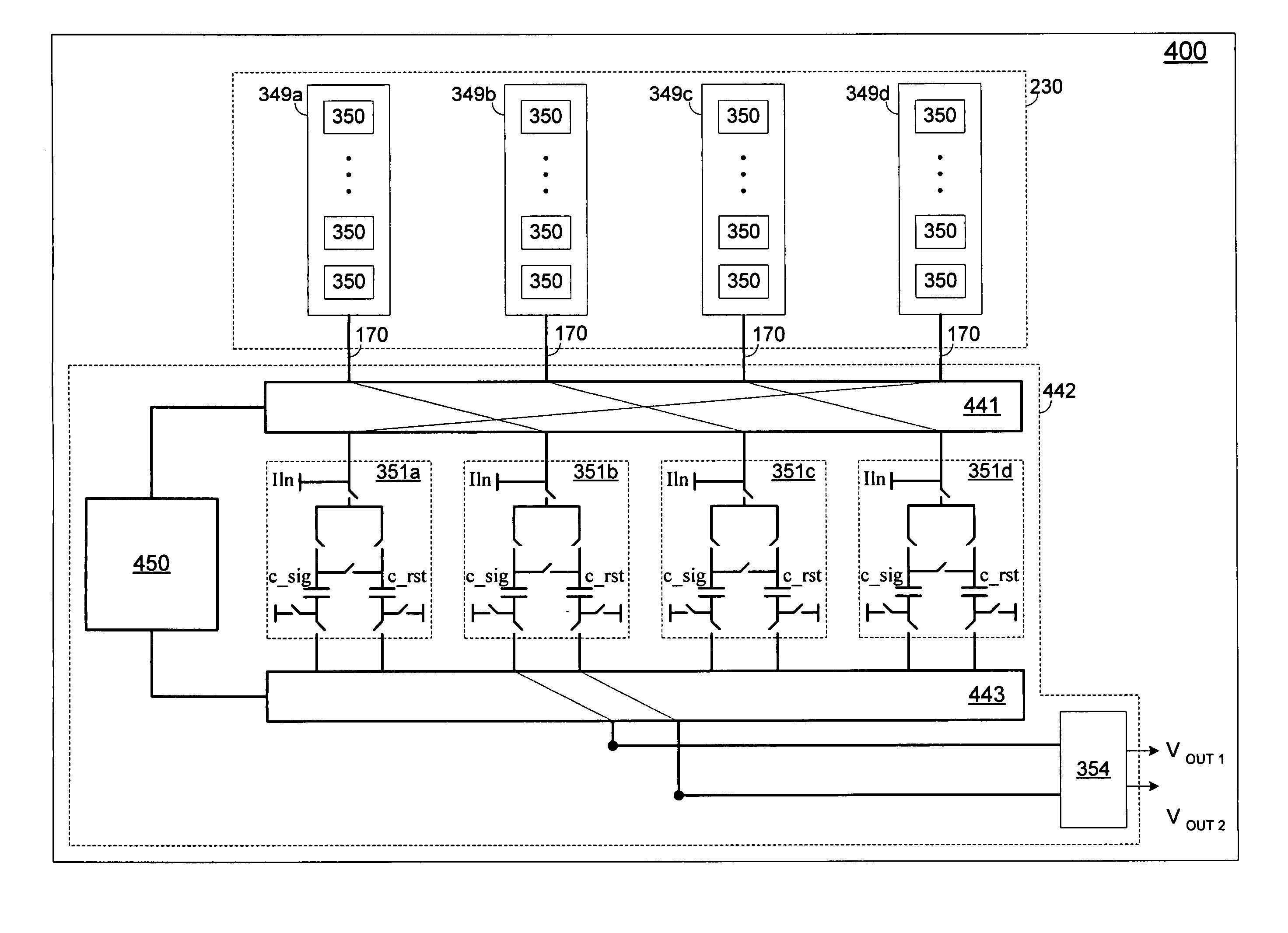
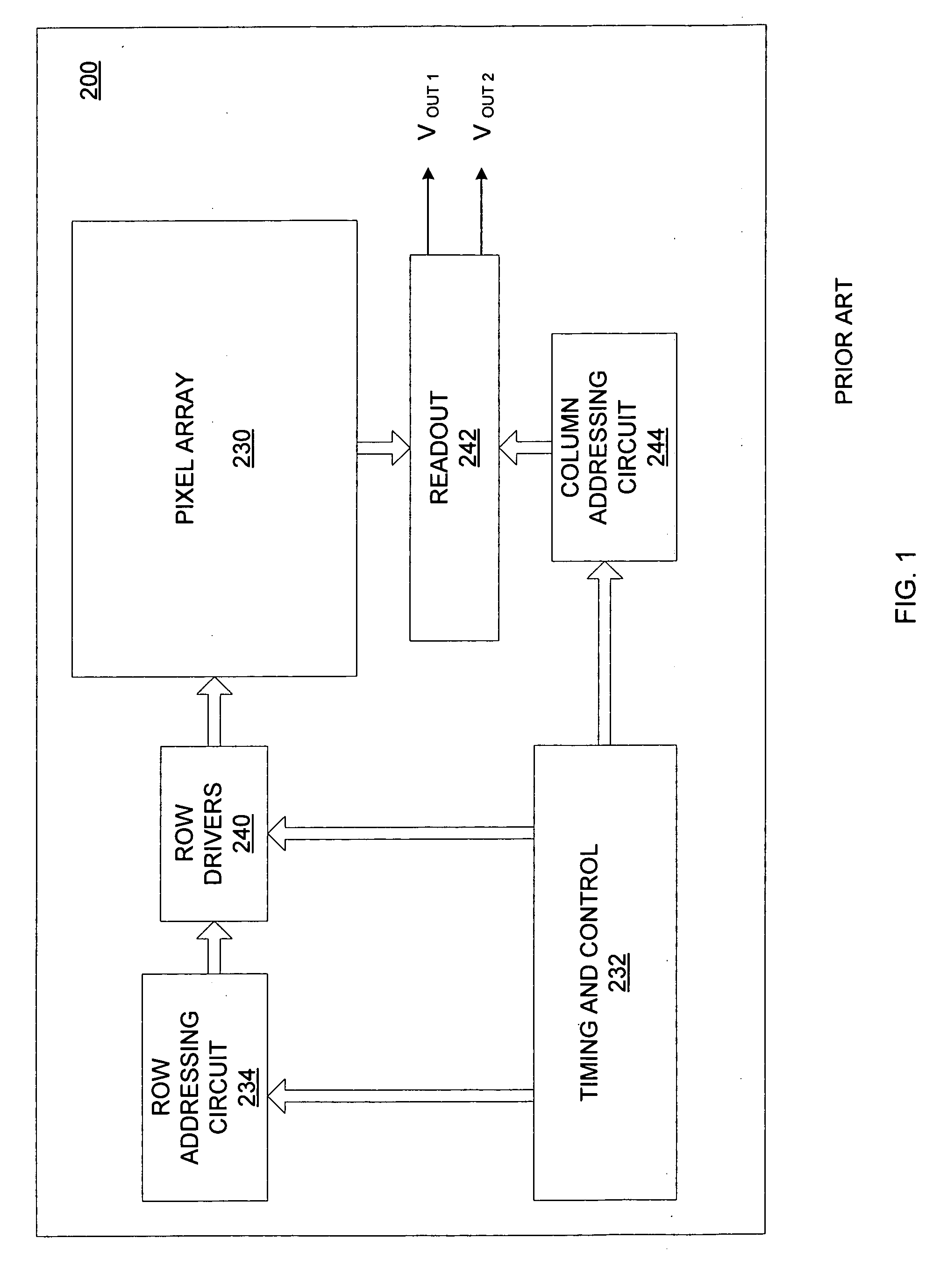
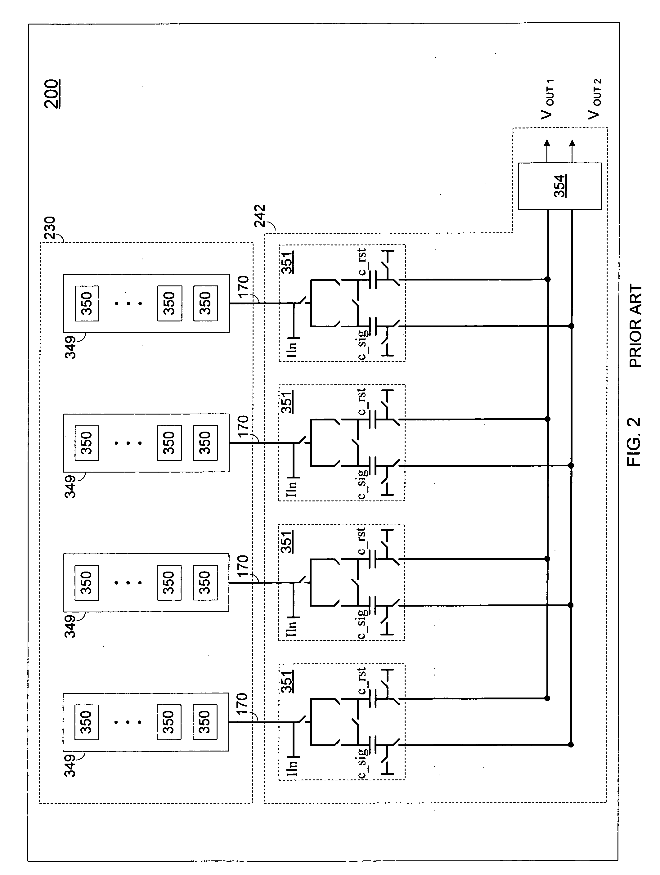
[0017]FIG. 3 depicts a signal processing system 400, which includes an active pixel sensor (“APS”) array 230 and a readout circuit 442 constructed in accordance with an exemplary embodiment of the invention. The signal processing system 400 differs from the system 200 illustrated in FIGS. 1 and 2 in several respects, which are described in greater detail below.

[0018] The illustrated system 400 includes pixel array 230 connected to the readout circuit 442. Read...


PUM


Abstract

An imager having a switching circuit that couples pixel columns to different sample and hold circuits to reduce the noticeability of column-wise fixed pattern noise. A controller randomly couples a pixel column to a sample and hold circuit, therefore fixed pattern noise emanating from a particular sample and hold circuit is not always associated with a single pixel column. Therefore the visual perception of fixed pattern noise associated with a particular sample and hold circuit is reduced.

Description

FIELD OF THE INVENTION [0001] The invention relates generally to semiconductor imaging devices, and more particularly to reducing the noticeability of fixed pattern noise in a solid state imager. BACKGROUND OF THE INVENTION [0002] There is a current interest in CMOS active pixel imagers for use as low cost imaging devices. Active pixel sensors can have one or more active transistors within the pixel unit cell, can be made compatible with CMOS technologies, and promise higher readout rates compared to passive pixel sensors. [0003]FIG. 1 shows a conventional imager 200 that includes an array of pixels 230 and a timing and control circuit or controller 232 which provides timing and control signals to control the reading out of signals stored in the pixels in a manner commonly known to those skilled in the art. Exemplary arrays have dimensions of M times N pixels, with the size of the array 230 depending on the particular application. The imager is read out a row at a time using a colum...

Claims


Application Information

Patent Timeline
Patent Type & Authority Applications(United States)
IPC IPC(8): H01L27/00H04N5/365H04N5/374H04N5/378
CPCH04N5/378H04N5/3658H04N25/677H04N25/75
Inventor YAN, HAI
Owner APTINA IMAGING CORP
Why Eureka
Try Eureka