
Decoding system for eight-to-fourteen modulation or eight-to-sixteen modulation
a decoding system and eight-to-fourteen-modulation technology, applied in the field of decoding, can solve the problems of increasing the design difficulty increasing the power consumption of the decoding chip, and increasing the read speed of dvd and cd drives, so as to eliminate the problems of increased power consumption and heat dissipation and avoiding the design complexity of the decoding chip
- Summary
- Abstract
- Description
- Claims
- Application Information
AI Technical Summary
Benefits of technology
Problems solved by technology
Method used
Image

Examples
Embodiment Construction
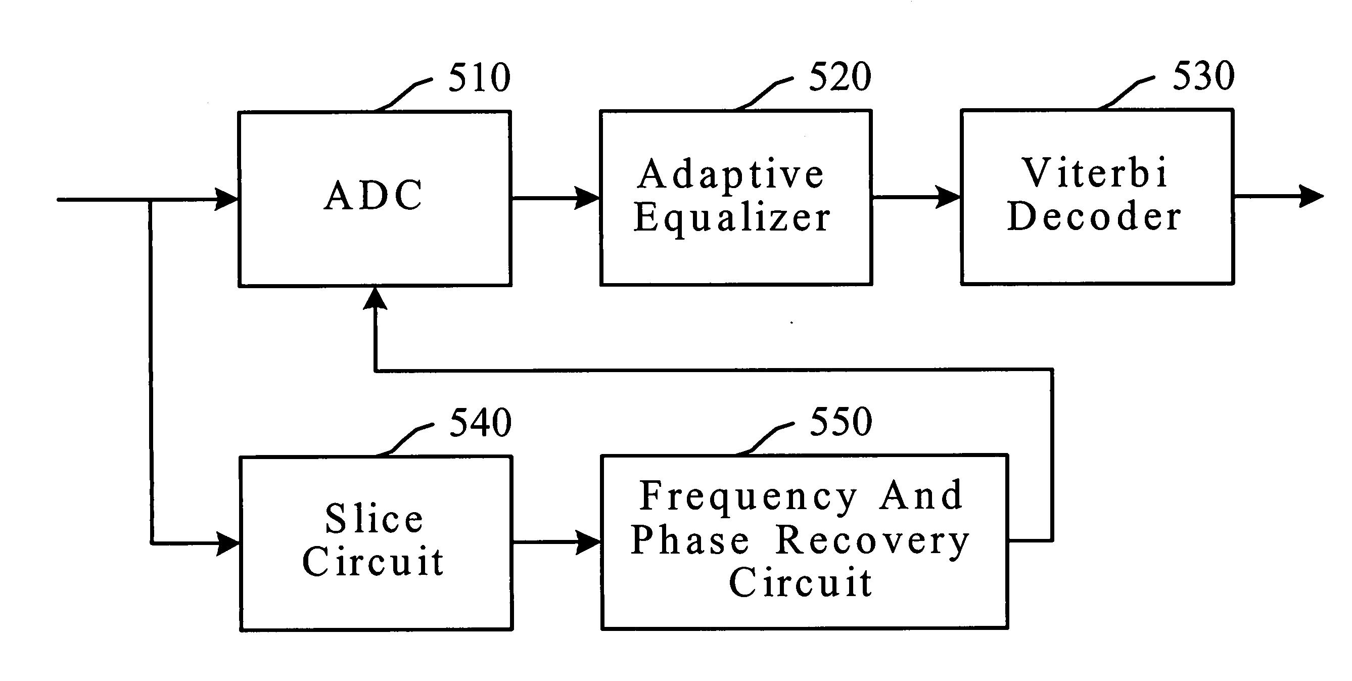
[0024]FIG. 5 is a block diagram of a decoding system for eight-to-fourteen modulation or eight-to-sixteen modulation (EFM / ESM) in accordance with the invention. As shown in FIG. 5, the system includes an analog to digital converter (ADC) 510, an adaptive equalizer 520, a Viterbi decoder 530, a slice circuit 540 and a frequency and phase recovery circuit 550.
[0025] As shown in FIG. 5, the ADC 510 receives an analog signal with an EFM or ESM feature, and converts the analog signal into a digital signal with the EFM or ESM feature. The slice circuit 540 has a hysteresis feature and detects a value of an input signal (the analog signal). Accordingly, the slice circuit 540 outputs a positive voltage when the value of the input signal is greater than a first hysteresis value, and outputs zero voltage when the value of the input signal is smaller than a second hysteresis value. The slice circuit 540 converts the analog signal into a second signal, which can be the positive voltage or zero...
PUM
 Abstract
Description
Claims
Application Information