
Local bias map using line width measurements

a local bias and line width technology, applied in the field of monitoring the production of photolithographic reticles, can solve the problems of reducing the yield of the fabrication line, adversely affecting the performance of the finished semiconductor device, and limiting the number of cd-sem sample sites

Inactive Publication Date: 2006-11-09
APPLIED MATERIALS INC
View PDF11 Cites 12 Cited by
  • Summary
  • Abstract
  • Description
  • Claims
  • Application Information

AI Technical Summary

Benefits of technology

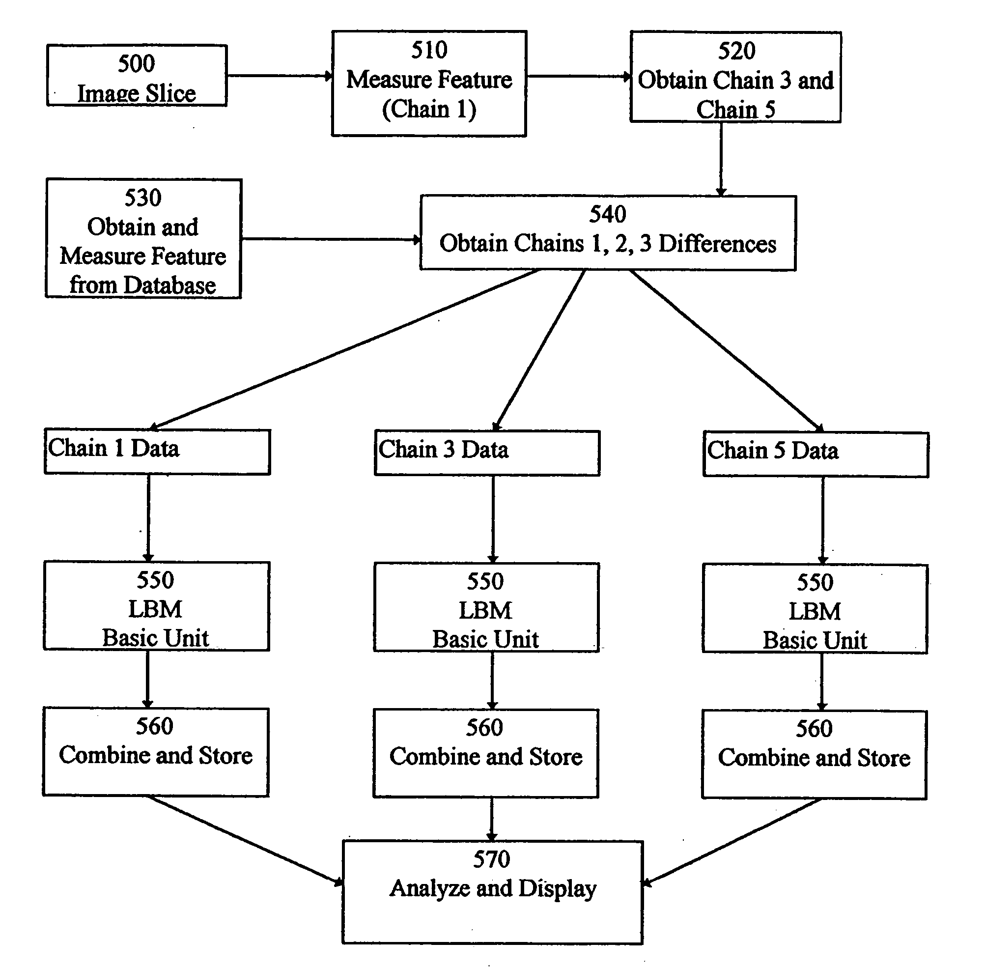
[0012] The present invention provides a solution for the need to inspect the entire reticle for CD deviations in addition to defect inspection. Two notable advantages of the invention are that: 1. it monitors CD over the entire reticle, and 2. it has no associated costs in terms of throughput, i.e., CD monitoring is done “on the fly” as the system inspects the reticle for defects.
[0013] According to a feature of the present invention, as the reticle inspection system scans the reticle for defects, various features on the reticle are being measured and compared against the database. Subsequently, in addition to a detect map, the system output a CD deviations map across the entire reticle. This enables fast and inexpensive method of

Problems solved by technology

Thus, any defect on the reticle would drastically reduce the yield of the fabrication line.
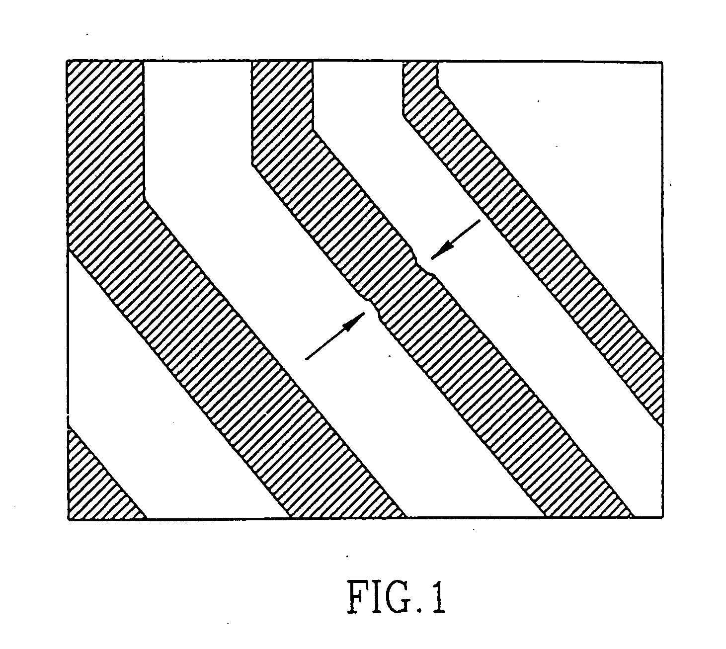
As design rules shrink and process windows (i.e., the margins for error in processing) become smaller, measurement of reticle features is becoming increasingly important, since even small deviations of line widths from design dimensions may adversely affect the performance of the finished semiconductor device.
Moreover, the number of CD-SEM sample sites is typically limited, since inspection time for each site is considerable.
Thus, significant but. unobvious CD errors may go unnoticed during inspection, such as “global” errors causing CD variations across the reticle, which indicate reticle manufacturing problems; e.g., a greater CD deviation in the features in the center of the reticle than in features at the perimeter of the reticle.
Specifically, perhaps the biggest technology issue in advancing optical lithography to smaller design rules is the Mask Error Factor ‘MEF’ a.k.a. mask error enhancement factor “MEEF’.

Method used


Image

  • Local bias map using line width measurements
  • Local bias map using line width measurements
  • Local bias map using line width measurements

Examples


Embodiment Construction

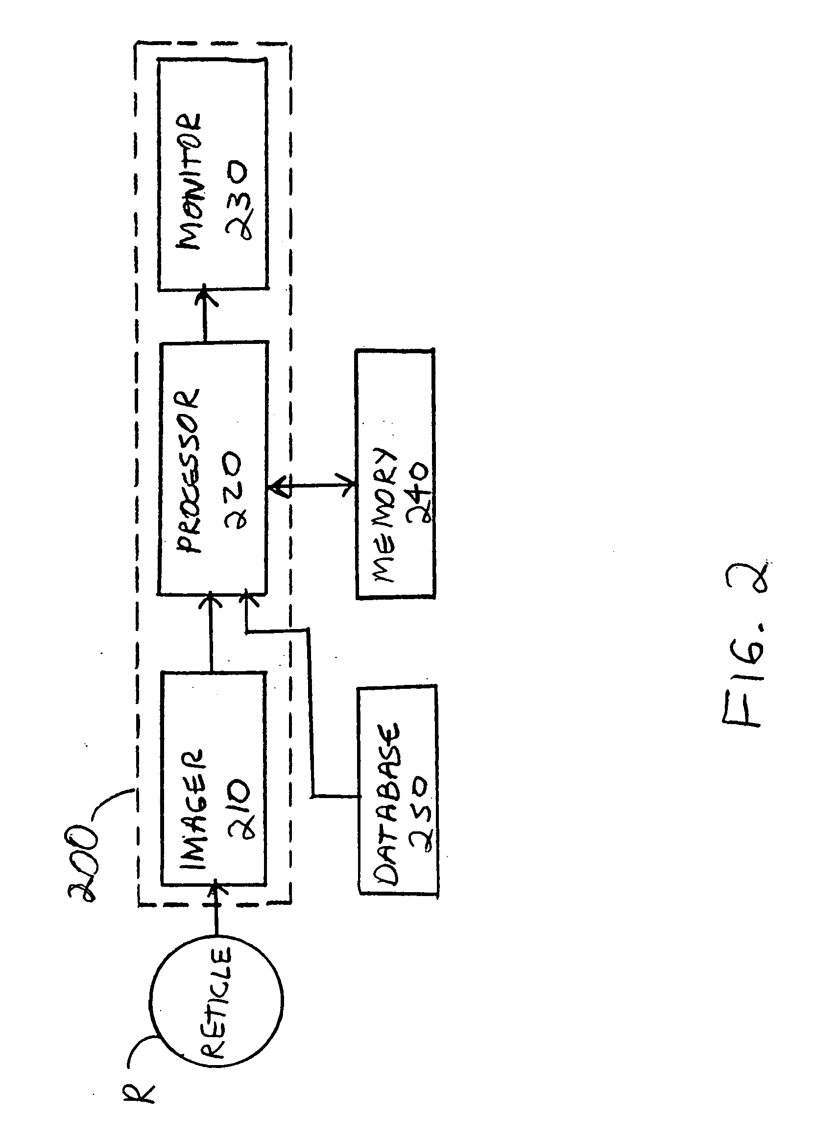
[0030] The present invention is implemented at an inspection tool 200, as shown in FIG. 2, comprising an imager 210 for imaging the surface of a reticle R at high speed, typically using a line or area CCD and an illumination source such as a lamp or a laser. Inspection tool 200 further comprises a processor 220, which preferably performs the analysis disclosed herein electronically, and a monitor 230 for displaying results of the analyses of processor 220. Processor 220 is in communication with a conventional reticle reference design database 250 and a memory device 240. Inspection tool 200 may be a conventional reticle inspection system, such as the RT-8200, ARIS-i, and the inspection tools described in U.S. Pat. No. 5,619,429, entitled “Apparatus and Method For Inspection Of a Patterned Object By Comparison Thereof To a Reference”, and U.S. Pat. No. 5,619,588, entitled “Apparatus and Method For Comparing and Aligning Two Digital Representations of an Image” the entire disclosures ...


PUM

PropertyMeasurementUnit
feature widthaaaaaaaaaa
thresholdaaaaaaaaaa
feature lengthaaaaaaaaaa

Abstract

A method and apparatus for inspecting a reticle measures line widths using an inspection tool that images the reticle and compares the image with a design database to detect errors in real time. The differences between the line widths of patterns on the reticle and the design database are stored during the inspection procedure. The difference (or “bias”) information is then processed off-line to create a map of all the local line-width deviation values (i.e., bias) of every feature on the reticle. The resultant local bias map can be used as a feedback mechanism to improve the reticle manufacturing process, as a “go / no go” criteria for the validity of the reticle, and as a standard report shipped together with the mask to the wafer fabrication facility, where it can be used as a yield-enhancing tool.

Description

RELATED APPLICATIONS [0001] This application a continuation of application Ser. No. 10 / 322,708, filed on Dec. 19, 2002, which is a continuation of application Ser. No. 09 / 286,498, filed on Apr. 5, 1999, the disclosures of which Applications are incorporated by reference herein.FIELD OF THE INVENTION [0002] The present invention relates to a method for monitoring the production of photolithographic reticles used in the manufacture of semiconductor devices, and more particularly for inspecting reticle. The invention has particular applicability for in-line inspection of reticles with submicron design features. BACKGROUND ART [0003] Current demands for high density and performance associated with ultra large scale integration require submicron features, increased transistor and circuit speeds and improved reliability. Such demands require formation of device features with high precision and uniformity, which in turn necessitates careful process monitoring. [0004] One important process ...

Claims


Application Information

Patent Timeline
Patent Type & Authority Applications(United States)
IPC IPC(8): G06K9/00G03F1/84G03F7/20G06T7/00
CPCG03F1/84G06T2207/30148G06T7/0006G03F7/70625
Inventor ERAN, YAIRGREENBERG, GADSADE, AMIHEMAR, SHIRLEY
Owner APPLIED MATERIALS INC
Learn More