

Semiconductor device and method for fabricating the same
a semiconductor device and bipolar transistor technology, applied in the direction of semiconductor devices, transistors, electrical equipment, etc., can solve the problems of not having a sufficient maximum oscillation frequency fsub>max/sub>, the actual doping technique using carbon as a base dopant has not been sufficiently established, and the ingaas-based hbts have very high maximum cut-off frequencies. achieve the effect of low base resistan
- Summary
- Abstract
- Description
- Claims
- Application Information
AI Technical Summary
Benefits of technology
Problems solved by technology
Method used
Image

Examples
first embodiment
A First Embodiment
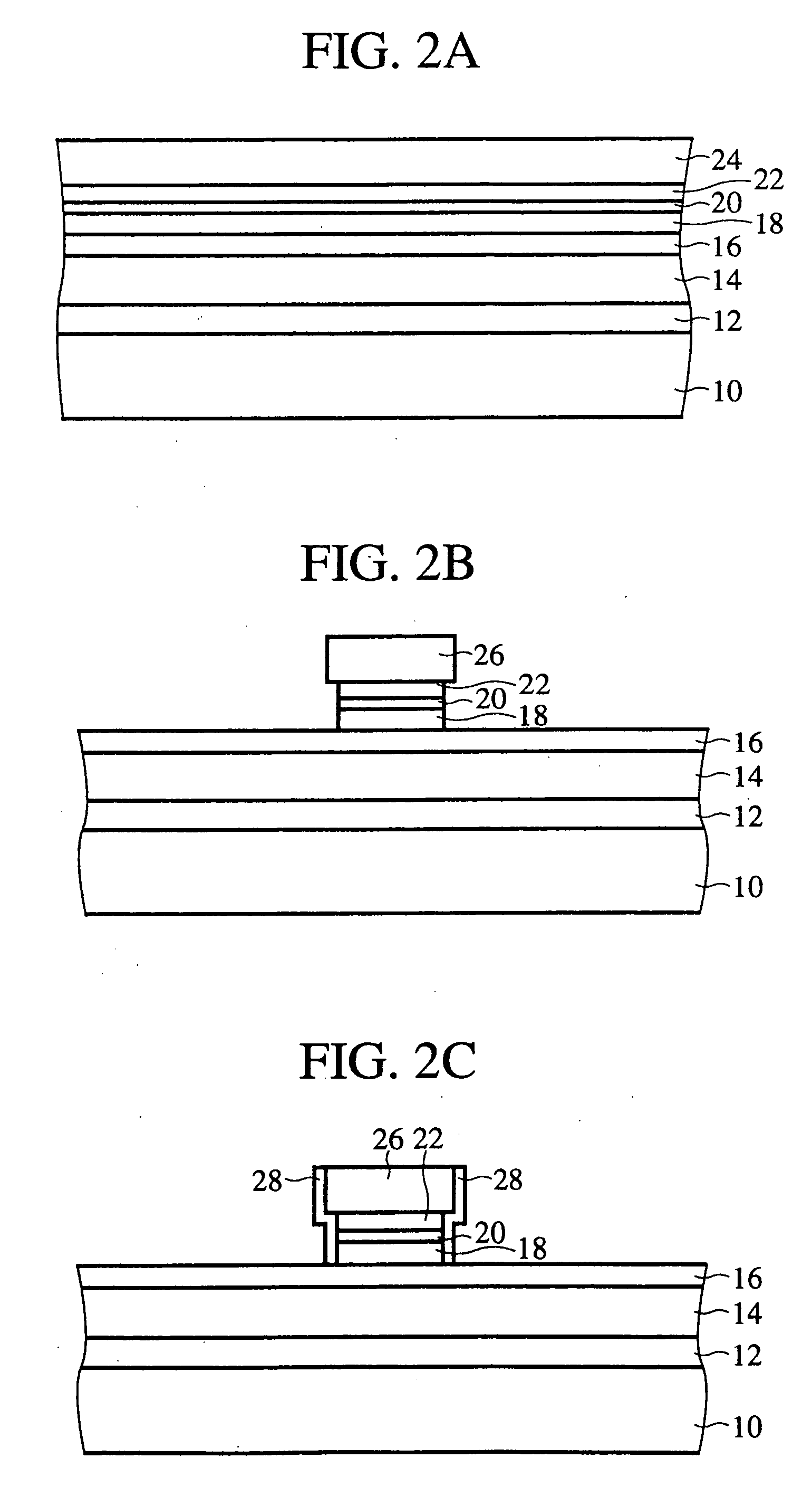
[0038] A semiconductor device and the method for fabricating the same according to a first embodiment of the present invention will be explained with reference to FIGS. 1, 2A-2C and 3A-3C.
[0039]FIG. 1 is a diagrammatic sectional view of the semiconductor device according to the present embodiment, which shows a structure thereof, and FIGS. 2A-2C and 3A-3C are sectional views of the semiconductor device according to the present embodiment in the steps of the method for fabricating the semiconductor device according to the present embodiment.
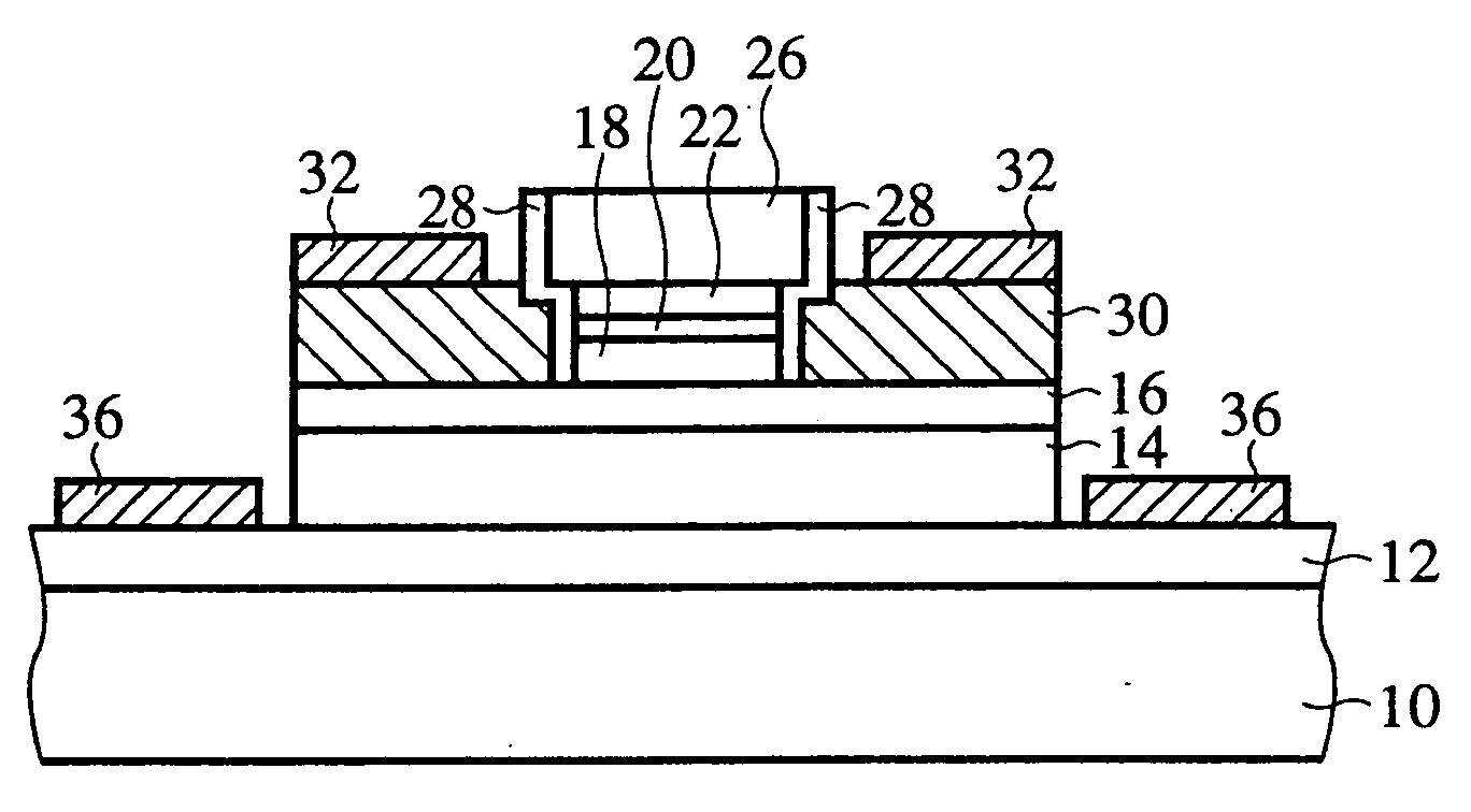
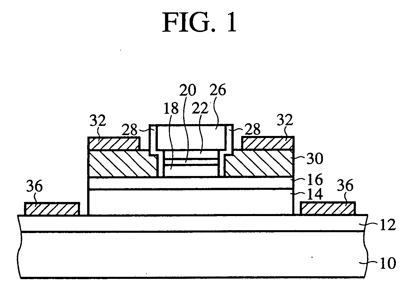
[0040] First, the structure of the semiconductor device according to the present embodiment will be explained with reference to FIG. 1.
[0041] A collector contact layer 12 of an n+-InGaAs layer is formed on a semi-insulating InP substrate 10. A collector layer 14 of an i-InGaAs layer is formed on the collector contact layer 12. A base layer 16 of a p+-InGaAs layer is formed on the collector layer 14. An emitter layer 18 of an n...
second embodiment
A Second Embodiment
[0067] The semiconductor device and a method for fabricating the same according to a second embodiment of the present invention will be explained with reference to FIGS. 4, 5A-5B and 6A-6C. The same members of the second embodiment as those of the semiconductor device and the method for fabricating the same according to the first embodiment are represented by the same reference numbers not to repeat or to simplify their explanation.
[0068]FIG. 4 is a diagrammatic sectional view of the semiconductor device according to the present embodiment, which shows a structure thereof. FIGS. 5A-5B and 6A-6B are sectional views of the semiconductor device in the steps of the method for fabricating the semiconductor device, which show the method.
[0069] In the present embodiment another semiconductor device having a decreased base resistance RB and the method for fabricating the same will be explained.
[0070] First, the structure of the semiconductor device according to the pre...
third embodiment
A Third Embodiment
[0080] A semiconductor device and a method for fabricating the same according to a third embodiment of the present invention will be explained with reference to FIGS. 7, 8A-8B and 9A-9B.
[0081]FIG. 7 is a diagrammatic sectional view of the semiconductor device according to the present embodiment, which shows a structure thereof. FIGS. 8A-8B and 9A-9B are sectional views of the semiconductor device according to the present embodiment in the steps of the method for fabricating the same, which show the method.
[0082] First, the structure of the semiconductor device according to the present embodiment will be explained with reference to FIG. 7.
[0083] The basic structure of the semiconductor device according to the present embodiment is the same as that of the semiconductor device according to the first embodiment shown in FIG. 1 but is characterized in that a surface passivation layer 38 of InP layer is formed on the base contact layer 30.
[0084] The surface passivati...
PUM
 Abstract
Description
Claims
Application Information