Trench gate power semiconductor field effect transistor

a technology of power semiconductor and field effect transistor, which is applied in the direction of transistors, basic electric elements, electric devices, etc., can solve the problems of inability to solve contact problems completely, the inability to reduce the on-resistance of those devices a lot, and the need for complex deposition and deep etching processes, so as to achieve high reliability and improve uis strength

Active Publication Date: 2016-12-22
JSAB TECH LTD
View PDF4 Cites 10 Cited by
  • Summary
  • Abstract
  • Description
  • Claims
  • Application Information

AI Technical Summary

Benefits of technology

[0009]Therefore, the object of the present invention is to provide a trench gate power MOSFET (TMOS) structure with reduced on-resistance.
[0010]To realize this and other objects, provided in the present invention is a TMOS structure with a heavily doped polysilicon source region. FIG. 5 shows the cross section of the device structure. As shown in the figure, the polysilicon n+ source region (11) has a depth (thickness) much larger than that of a conventional TMOS, and can provide a relatively lower contact resistance on the side wall of the n+ source region (11) compared with the conventional TMOS The polysilicon n+ source region (11) can be formed by low-temperature deposition after the p-type body region (13) is formed. Therefore, the doping profile of the p-type body region (13) can be well controlled, since it is formed near the surface of silicon. On the other hand, compared with the cell pitch of the device shown in FIG. 1, the trench-shaped contact hole at the source of the device provides a reduced cell pitch. Through the use of the trench-shaped contact hole, the polysilicon n+ source region (11) is contacted by the source electrode (22) on the side wall of the contact hole, and if the cell pitch is further decreased by using more advanced photolithography, the contact resistance will not increase. In addition, the trench-shaped contact hole also provides a low base resistance of the parasitic n+ source region (11) / P-type body region (13) / n—epi (14) bipolar junction transistor (BJT), thereby giving the device a more rugged UIS performance [5].
[0011]In addition, the present invention may also be implemented in a trench gate IGBT structure to provide reduced on-state drop and latch-up free feature.

Problems solved by technology

However, a complicated deposition and deep etching process is required to form the ILD (32) in the device.
Due to such restriction, even if the advanced photolithography technology is used, the on-resistance of those devices still cannot be reduced a lot.
However, in the buried gate structure, the contact area is still restricted by the cell pitch, and contact problems cannot be solved completely.
However, if the n+ source region (11) is relatively deep, high-energy ion implantation is required to form the p-type body region (13), and it is difficult to realize approximately uniform doping profile due to the relatively large standard deviation of the implanted projected range.

Method used


Image

  • Trench gate power semiconductor field effect transistor
  • Trench gate power semiconductor field effect transistor
  • Trench gate power semiconductor field effect transistor

Examples


Embodiment Construction

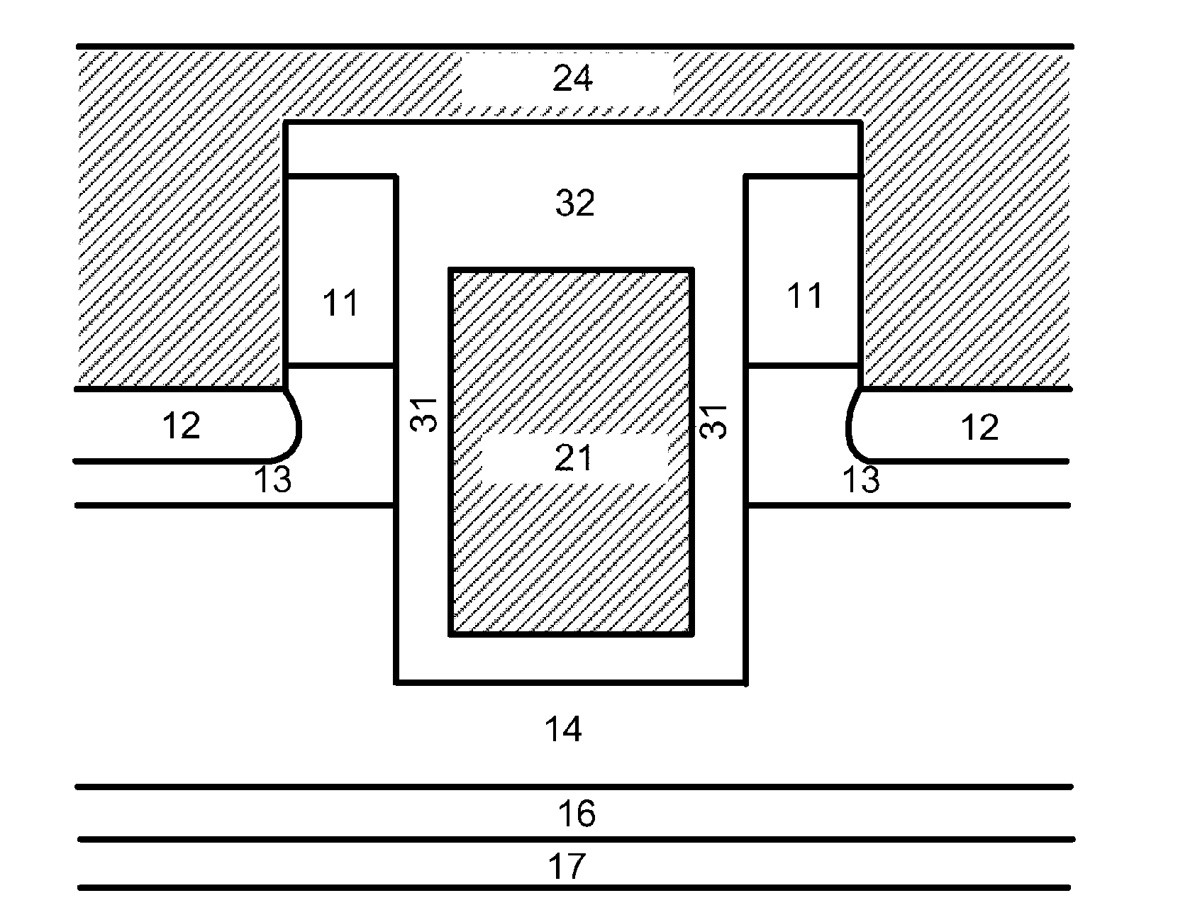
[0124]FIG. 1 is a cross sectional view of a TMOS structure in the prior art. In the device, about half of an n+ source region (11) is covered by an interlayer dielectric (ILD) (32), and the remaining n+ source region (11) is contacted by a source electrode (22). The source electrode (22) is isolated from a gate electrode (21) by the ILD (32).

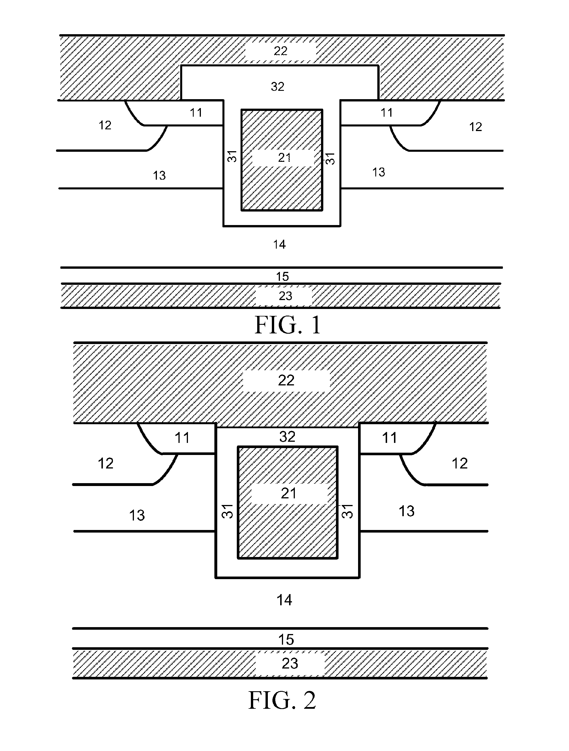
[0125]FIG. 2 is a cross sectional view of a trench gate TMOS structure in the prior art. In the device, all of the ILD (32) is located in a trench, and the whole upper surface of the n+ source region (11) is contacted by the source electrode (22).

[0126]FIG. 3 is a cross sectional view of a buried gate TMOS structure in the prior art. In the device, all of the ILD (32) is located in a trench, and the whole upper surface of the n+ source region (11) is contacted by the source electrode (22). In addition, part of the n+ source region (11) is located on the top of the ILD (32), and this part of n source region (11) is polysilicon.

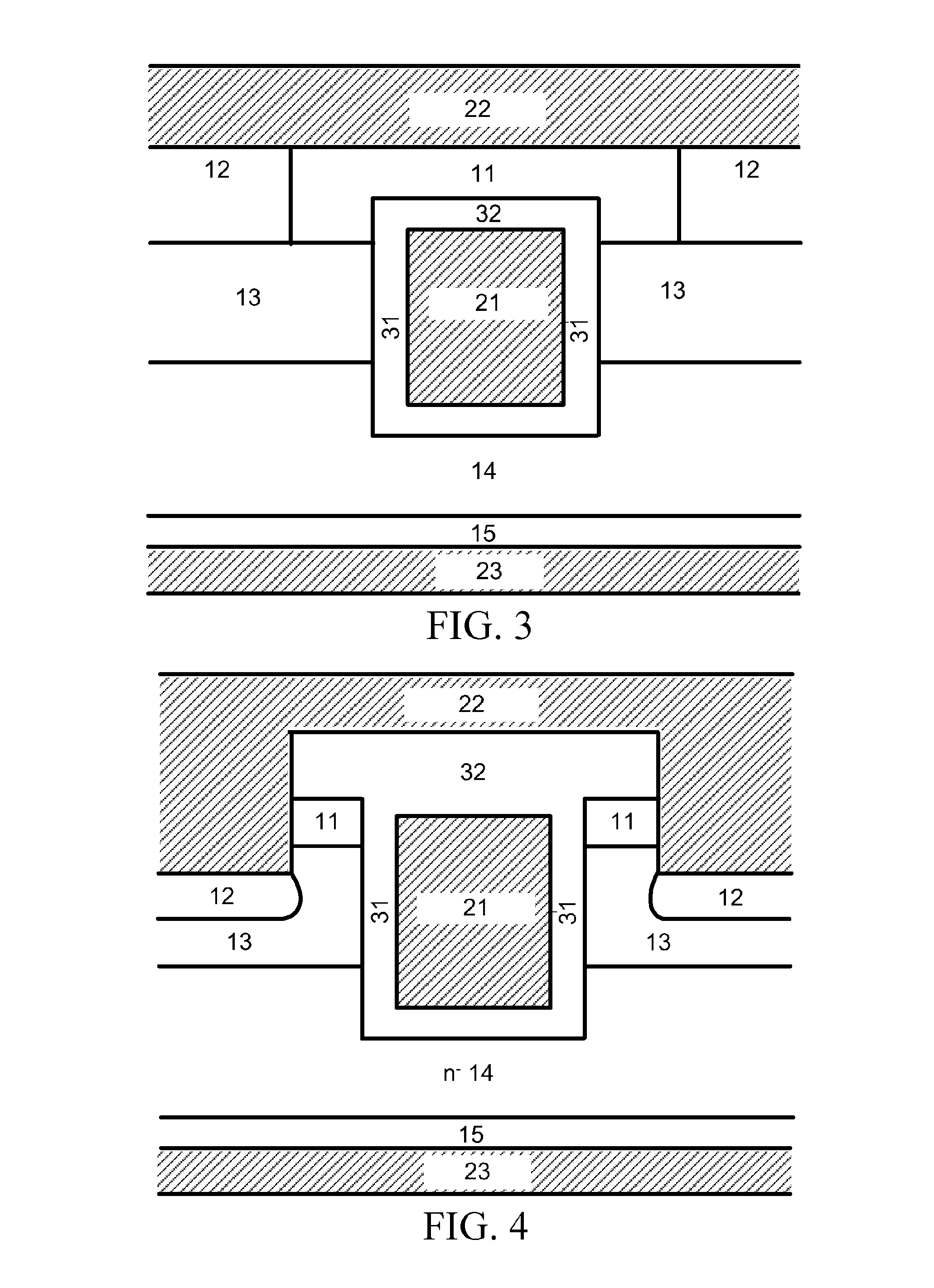
[0127]FIG. 4 is a c...


PUM


Abstract

Provided in the present invention is a trench gate power MOSFET (TMOS / UMOS) structure with a heavily doped polysilicon source region. The polysilicon source region is formed by deposition, and a trench-shaped contact hole is used at the source region, in order to attain low contact resistance and small cell pitch. The present invention may also be implemented in an IGBT.

Description

BACKGROUNDTechnical Field[0001]The present invention generally relates to a structure and manufacturing of power field effect transistors, and specifically relates to a trench gate power metal oxide semiconductor field effect transistor (MOSFET) and a trench gate insulated gate bipolar transistor (IGBT).Related Art[0002]The present invention will be described in an n channel power FET, but it will be appreciated in the following description that the present invention is also applicable to a p channel power FET. In the specification of the present invention, heavily doped n-type regions are labeled as n+ and heavily doped p-type regions are labeled as p+. These heavily doped regions usually have a doping concentration of between 1×1018 cm−3 and 1×1021 cm−3. On the other hand, lightly doped n-type regions are labeled as n- and lightly doped p-type regions are labeled as p−. These lightly doped regions usually have a doping concentration of between 1×1013 cm−3 and 1×1017 cm−3.[0003]Low...

Claims


Application Information

Patent Timeline
Patent Type & Authority Applications(United States)
IPC IPC(8): H01L29/66H01L29/10H01L29/06H01L21/3065H01L21/265H01L21/324H01L21/285H01L29/739H01L29/08
CPCH01L29/66348H01L29/7397H01L29/1095H01L29/0649H01L21/3065H01L29/0821H01L21/265H01L21/324H01L21/28556H01L29/0804H01L29/0856H01L29/41766H01L29/66295H01L29/66333H01L29/6634H01L29/66727H01L29/66734H01L29/78H01L29/7813
Inventor FUNG, SHUK-WAZHOU, XIANDASIN, JOHNNY KIN ON
Owner JSAB TECH LTD
Why Eureka
Try Eureka