Semiconductor device and hetero-junction bipolar transistor

a technology of semiconductor devices and bipolar transistors, applied in the direction of semiconductor devices, basic electric elements, electrical appliances, etc., can solve the problems of inability to completely inhibit the generation of strains, crystallinity, and difficulty in fabricating quality hbts, so as to improve the high-frequency characteristics, reduce the resistance in the second semiconductor layer, and reduce the resistance

Active Publication Date: 2005-06-09
PANASONIC CORP
View PDF3 Cites 9 Cited by
  • Summary
  • Abstract
  • Description
  • Claims
  • Application Information

AI Technical Summary

Benefits of technology

[0067] According to the invention of claim 16, a thin layer portion is formed so that the interface with the first semiconductor layer is left in the second semiconductor layer and an electrode for taking out electrons in the second semiconductor layer is in contact with the thin layer portion. Thus, due to the internal electric field generated in the second semiconductor layer, holes are stored in the vicinity of the interface with the first semiconductor layer in the thin layer portion. As a result, holes are stored in the vicinity of the electrode in contact with the thin layer portion of the second semiconductor layer, so that a resistance in the second semiconductor layer can be reduced.
[0068] According to the invention of claim 17, the contact layer of n-type GaN is in contact with the first semiconductor layer and the first semiconductor layer and the electrode for injecting electrons into the first semiconductor layer form an ohmic contact with the contact layer interposed therebetween, so that conduction electrons are stored in the contact layer side of the interface of the first semiconductor layer and the contact layer. Thus, conduction electrons can be used for forming an ohmic contact with the electrode and a low resistance ohmic contact can be formed. Therefore, high-frequency characteristics can be improved.
[0069] According to the invention of claim 18, the contact layer of n-type GaN is in contact with the first semiconductor layer, a thin layer portion is formed so that the interface with the contact layer is left, and the electrode is in contact with the thin layer portion. Thus, conduction electrons are stored in the contact layer side of the interface of the thin layer portion of the first semiconductor layer and the contact layer. Therefore, the conduction electrons can be used for forming an ohmic contact with the electrode and a low resistance ohmic contact can be formed. Therefore, high-frequency characteristics can be improved.
[0070] According to the invention of claim 20, a base layer of an HBT is formed of GaN and the base layer is in contact with an emitter layer at its nitrogen polarity surface while being in contact with the collector layer at its gallium polarity surface. Thus, an internal electric field can be generated in the base layer so that electrons as carriers are accelerated in the direction from the emitter layer to the collector layer. Therefore, the transit time of electrons can be reduced, so that high-frequency characteristics can be improved. Moreover, due to the internal electric field, holes can be stored in the vicinity of the base electrode, so that a base resistance can be reduced. Furthermore, there is no need to change the composition ratio of the base layer in the film thickness direction. As a result, it is possible to prevent a fabrication method from becoming complicated and also to stably obtain a quality HBT.
[0071] According to the invention of claim 21, each of the emitter layer and the collector layer is formed of AlGaN. Thus, a very large electric charge is generated at the interface of the emitter layer and the base layer and a very large internal electric field can be generated in the base layer. As a result, the transit time of electrons in the base layer can be efficiently and reliably reduced. Furthermore, the interface of the emitter layer and the base layer is a hetero-junction, so that the efficiency of injection into the base layer can be improved.
[0072] According to the invention of claim 22, the emitter layer is formed of AlGaN and the collector layer is formed of GaN. Thus, a sufficiently large electric charge is generated at each interface and a sufficiently large internal electric field can be formed in the base layer. As a result, the transit time of electrons in the base layer can be efficiently and reliably reduced. Furthermore, in the present invention, a barrier is not generated at the interface of the base layer and the collector layer. Also in this point, the transit time of carriers can be reduced, so that high-frequency characteristics can be improved.

Problems solved by technology

However, it is not possible to completely inhibit the generation of strains and therefore a piezo polarization is generated.
Thus, not only a fabrication method becomes complicated but also it is difficult, in view of crystallinity, to fabricate a quality HBT.

Method used


Image

  • Semiconductor device and hetero-junction bipolar transistor
  • Semiconductor device and hetero-junction bipolar transistor
  • Semiconductor device and hetero-junction bipolar transistor

Examples


embodiment 1

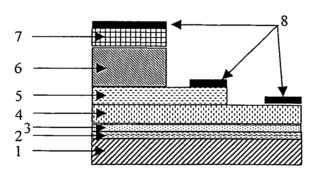
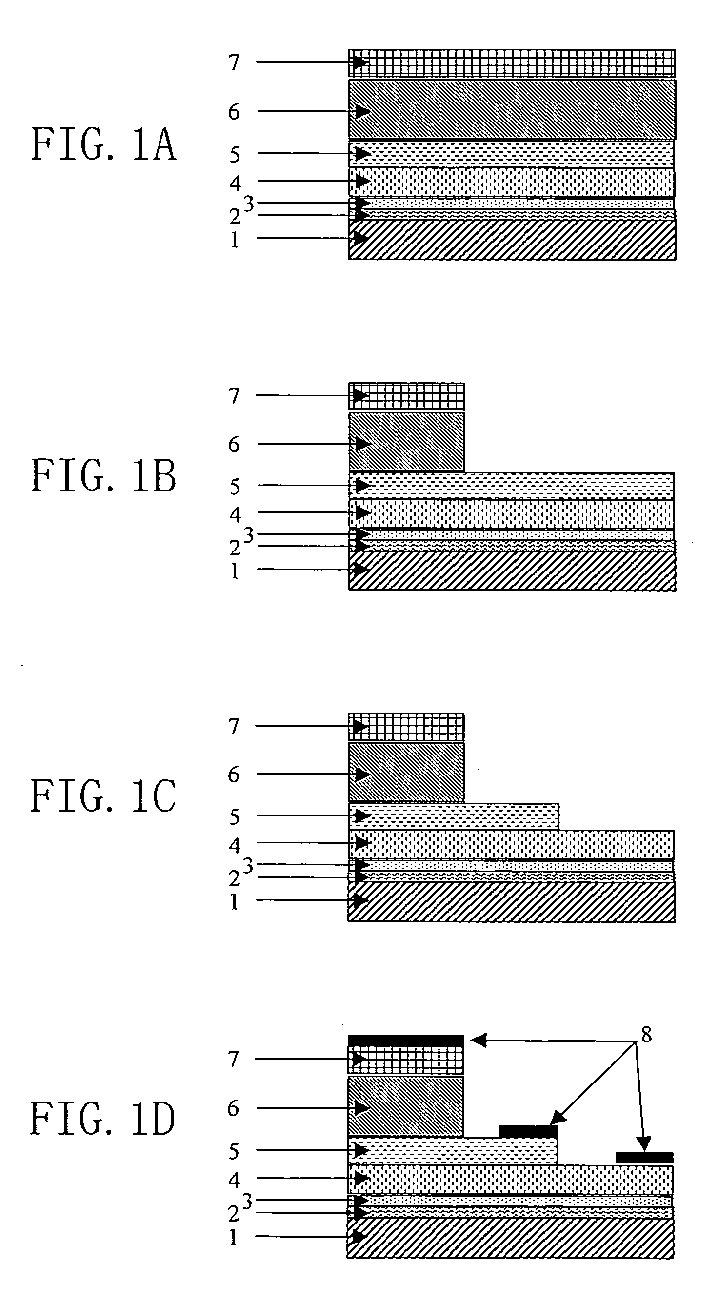
[0084] As shown in FIG. 1, a semiconductor device according to EMBODIMENT 1 is formed as a hetero-junction bipolar transistor (HBT) in which an emitter layer 4 as a first semiconductor layer, a base layer 5 as a second semiconductor layer, and a collector layer 6 as a third semiconductor layer are formed over a sapphire substrate 1. Each of the layers is formed by metal organic chemical deposition (MOCVD).

[0085] On the sapphire substrate 1, an AlN buffer layer 2 of aluminum nitride (AlN) is formed. The AlN buffer layer 2 is formed so as to have a thickness of 20 nm. On the AlN buffer layer 2, a GaN buffer layer 3 of gallium nitride (GaN) is formed. The GaN buffer layer 3 is formed so as to have a thickness of 15 nm. The GaN buffer layer 3 is formed by MOCVD and thus a surface (upper surface) thereof at a time when the GaN buffer layer is formed is a gallium polarity surface in which gallium is located at the outermost side. Moreover, an interface (lower surface) of the GaN buffer l...

second embodiment

[0104]FIG. 4 illustrates EMBODIMENT 2 of the present invention. In this embodiment, each member also described in EMBODIMENT 1 is identified by the same reference numeral and the detailed description thereof will be omitted. In EMBODIMENT 1, a so-called collector-up structure in which the configuration in which the emitter layer 4, the base layer 5 and the collector layer 6 are stacked in this order from the substrate 1 side is formed. In contrast, in EMBODIMENT 2, an emitter-up structure in which the collector layer 6, the base layer 5 and the emitter layer 4 are stacked in this order from the substrate 1 side is formed. Each of the layers is formed by molecular beam epitaxy (MEB).

[0105] The GaN buffer layer 3 is formed by MBE. Thus, a surface (upper surface) of the GaN buffer layer 3 at a time when the GaN buffer layer 3 is formed is a nitrogen polarity surface in which nitrogen is located at the outermost side. Moreover, an interface (lower surface) of the GaN buffer layer 3 wit...

third embodiment

[0119]FIG. 5 illustrates EMBODIMENT 3 of the present invention. In this embodiment, each member also described in EMBODIMENT 1 is identified by the same reference numeral and therefore the detailed description thereof will be omitted. In EMBODIMENT 3, a collector-up structure is formed and a heavily doped layer 9 is provided in the collector layer 6.

[0120] The heavily doped layer 9 is formed by δ doping. That is, only monosilane (SiH4) is introduced into a furnace when the collector layer 6 has been formed to have a thickness of 20 nm or less, and more preferably a thickness of 10 nm or less, i.e., for example, a thickness of 3 nm, thereby forming the heavily doped layer 9 doped with Si at a high concentration (5×1012 cm−2). Thereafter, the collector layer 6 is formed again so that the thickness the collector layer 6 becomes 500 nm. Thus, in the collector layer 6, the heavily doped layer 9 doped with an impurity at a high concentration is provided only in part of the collector laye...


PUM


Abstract

In an npn-type HBT, each of an emitter layer and a collector layer is formed of AlGaN and a base layer is formed of GaN. The emitter layer is in contact with a nitrogen polarity surface of the base layer and the collector layer is in contact with a gallium polarity surface of the base layer. An electric charge is generated at each interface due to a spontaneous polarization and a piezo polarization generated in each of the layers. Because of the electric charge, an internal field is generated so as to accelerate electrons in the base layer.

Description

CROSS-REFERENCE TO RELATED APPLICATION [0001] This application claims priority under 35 U.S.C. § 119(a) on Japanese Patent Application No. 2003-309586 filed on Sep. 2, 2003, the entire contents of which are hereby incorporated by reference. BACKGROUND OF THE INVENTION [0002] 1. Technical Field to which the Invention Belongs [0003] The present invention relates to a semiconductor device and a hetero-junction bipolar transistor in which an n-type first semiconductor layer, a p-type second semiconductor layer and an n-type third semiconductor layer are in contact with one another in this order, and more particularly relates to measures for improving high-frequency characteristics. [0004] 2. Prior Art [0005] Conventionally, nitride semiconductor has been well known. The known nitride semiconductor is a semiconductor which has a wide band gap and a high breakdown electric field and therefore its high output operation has been expected. As semiconductor devices using this nitride semicond...

Claims


Application Information

Patent Timeline
Patent Type & Authority Applications(United States)
IPC IPC(8): H01L21/331H01L29/20H01L29/737
CPCH01L29/2003H01L29/7371H01L29/66318
Inventor NAKAZAWA, SATOSHIHIROSE, YUTAKATANAKA, TSUYOSHI
Owner PANASONIC CORP
Why Eureka
Try Eureka