Optical element, optical device, mobile information terminal, and manufacturing method
- Summary
- Abstract
- Description
- Claims
- Application Information
AI Technical Summary
Benefits of technology
Problems solved by technology
Method used
Image
Examples
Embodiment Construction
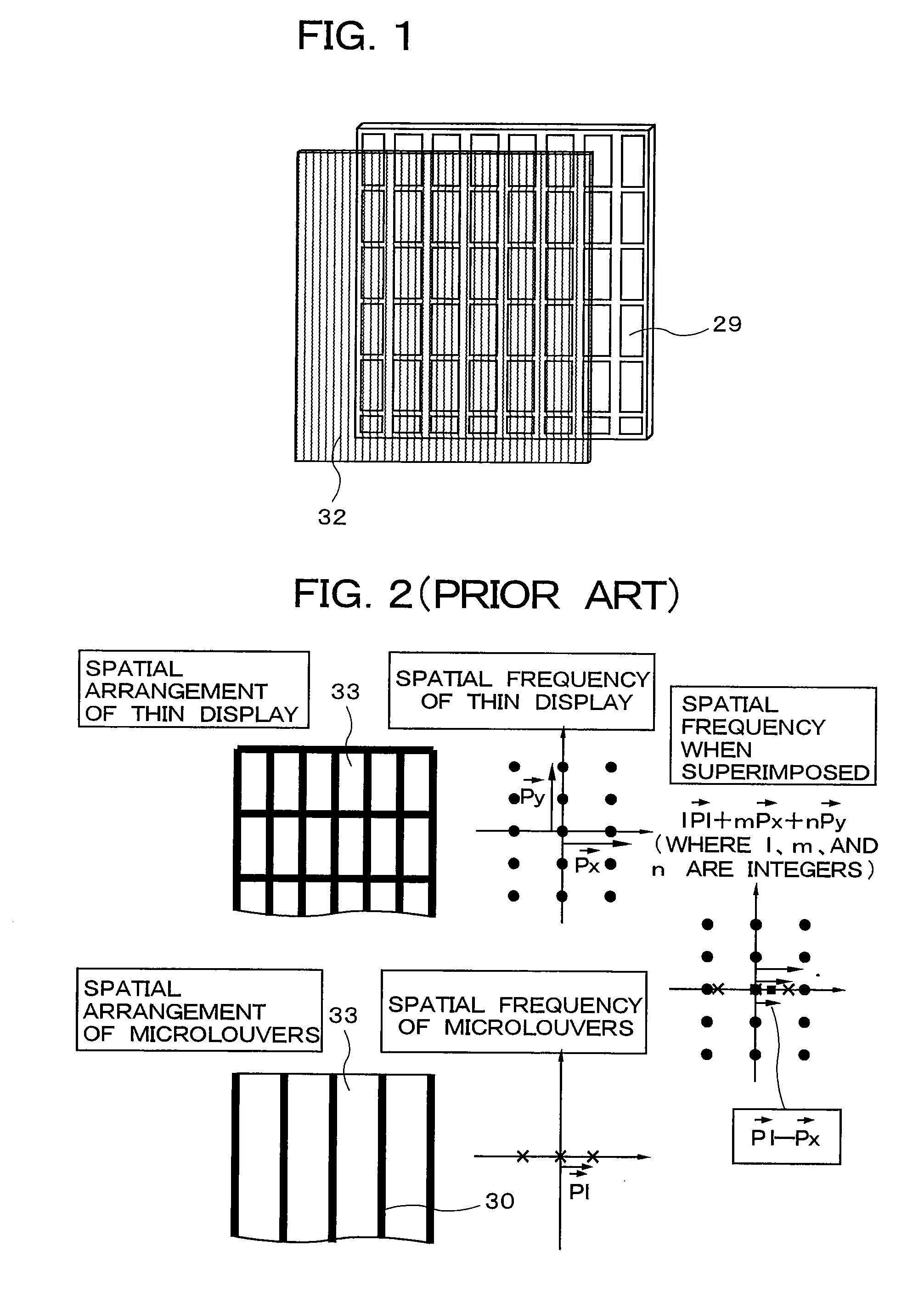
[0050] Embodiments of the present invention are described in detail below with reference to the attached diagrams. FIG. 1 is a view of a microlouver 32 mounted on a display panel 29 in the first embodiment of the present invention. The microlouver 32 of the present embodiment is configured so that light-absorbing layers and transparent layers are disposed in an irregular and alternating manner.
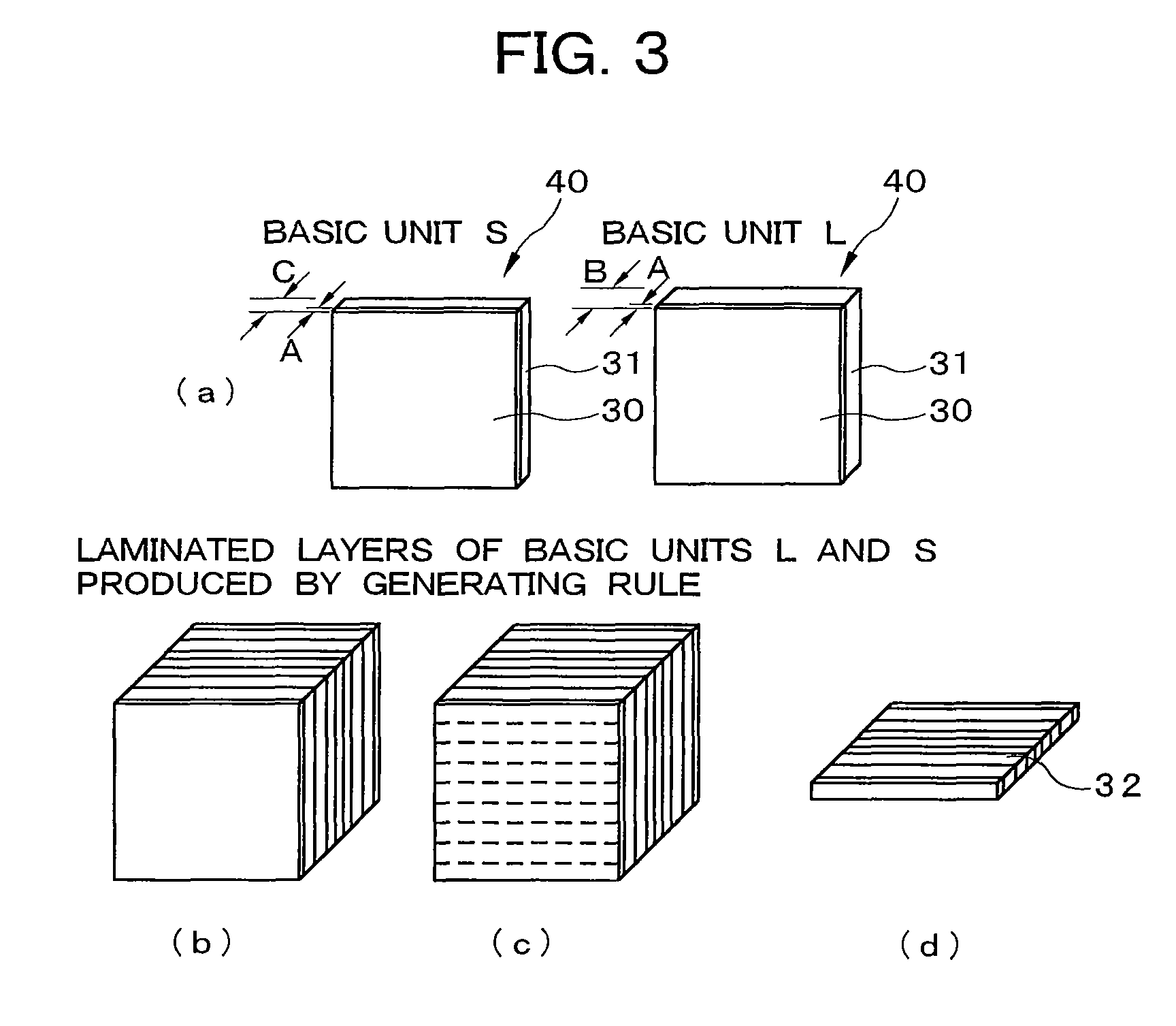
[0051]FIGS. 3A to 3D are views showing the method of manufacturing the microlouver. First, a plurality of two types of light-controlling layers 40 in which a light-absorbing layer 30 is laminated on a transparent layer 31 are prepared, as shown in FIG. 3A. The light-controlling layer 40 of the basic unit L has a light-absorbing layer 30 with a thickness of A, and a transparent layer 31 with a thickness of B. The light-controlling layer 40 of the basic unit S has a light-absorbing layer 30 with a thickness of A and a transparent layer 31 with a thickness of C (C≠B).
[0052] The light-controllin...
PUM
 Abstract
Description
Claims
Application Information


