Method and apparatus providing integrated color pixel with buried sub-wavelength gratings in solid state imagers

Active Publication Date: 2007-03-01
APTINA IMAGING CORP
View PDF34 Cites 34 Cited by
  • Summary
  • Abstract
  • Description
  • Claims
  • Application Information

AI Technical Summary

Benefits of technology

[0026]FIG. 12 is an illustration of an imaging system having an imager with reduced

Problems solved by technology

This greatly reduces the overall efficiency of the image sensor.
Moreover, the color mosaic required for this techni

Method used


Image

  • Method and apparatus providing integrated color pixel with buried sub-wavelength gratings in solid state imagers
  • Method and apparatus providing integrated color pixel with buried sub-wavelength gratings in solid state imagers
  • Method and apparatus providing integrated color pixel with buried sub-wavelength gratings in solid state imagers

Examples


Example

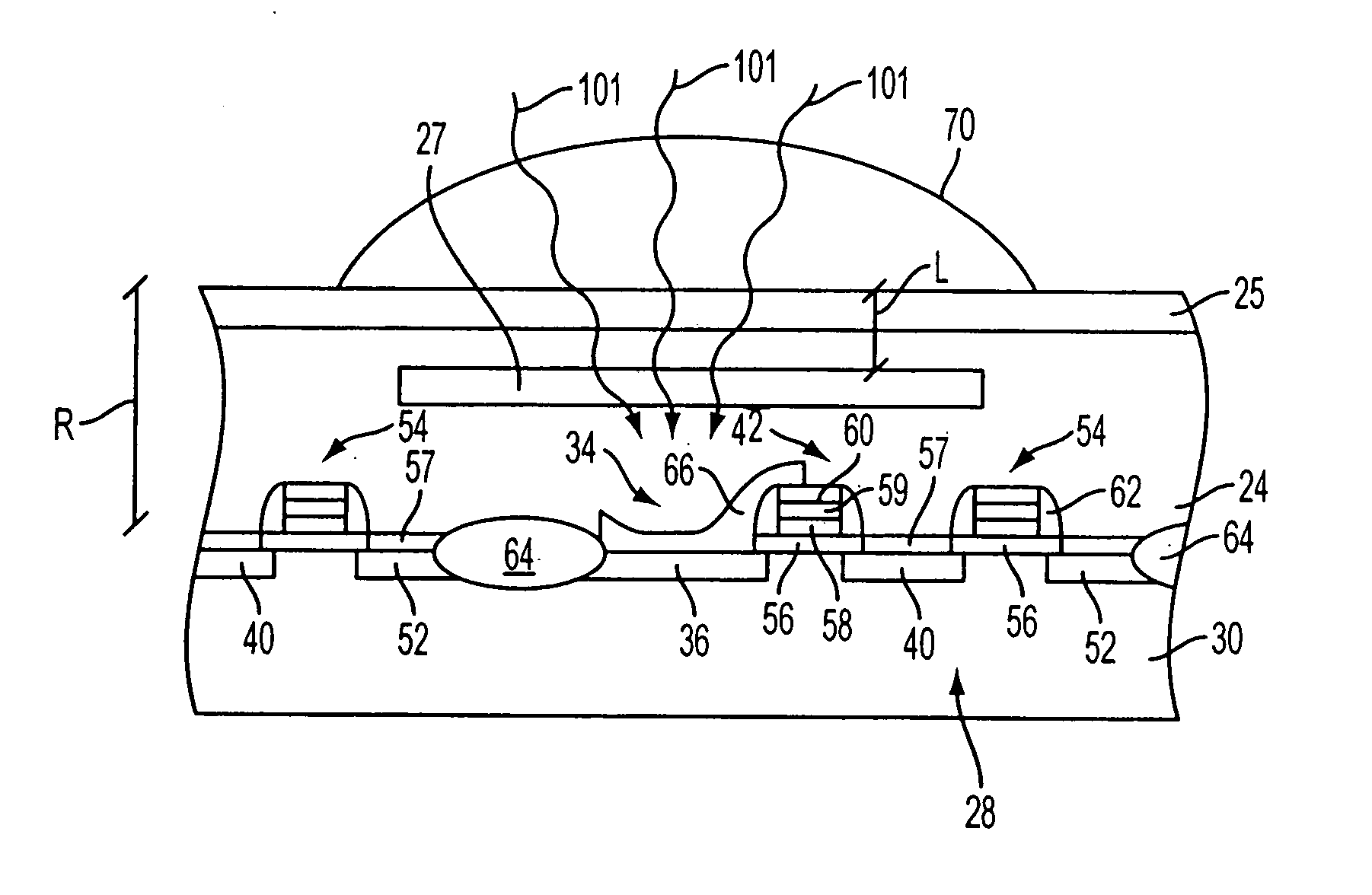
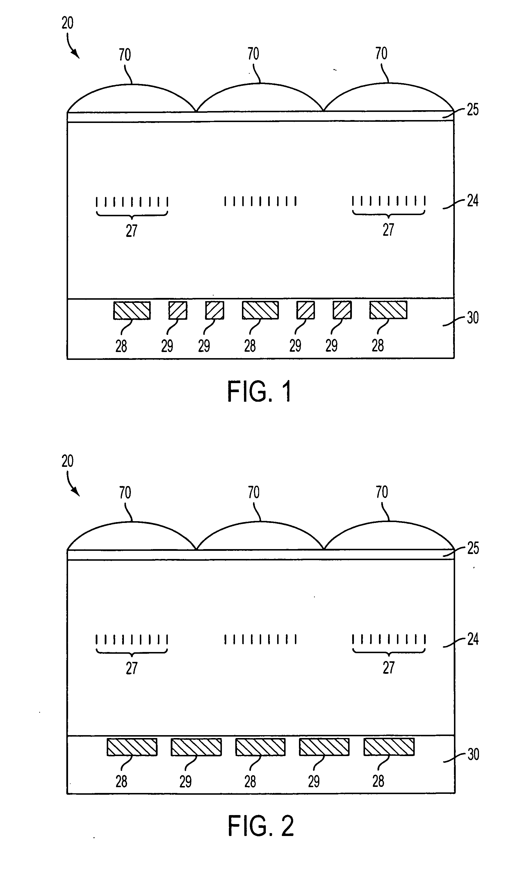
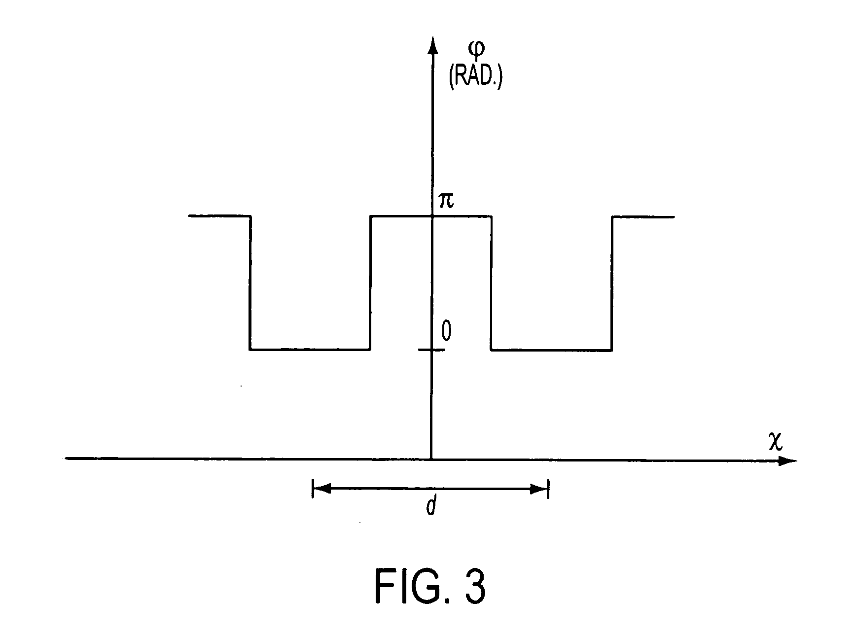
[0027] In the following detailed description, reference is made to the accompanying drawings, which form a part hereof and show by way of illustration specific embodiments in which the invention may be practiced. These embodiments are described in sufficient detail to enable those skilled in the art to practice the invention, and it is to be understood that other embodiments may be utilized, and that structural, logical, and electrical changes may be made without departing from the spirit and scope of the present invention. The progression of processing steps described is exemplary of embodiments of the invention; however, the sequence of steps is not limited to that set forth herein and may be changed as is known in the art, with the exception of steps necessarily occurring in a certain order.

[0028] The term “substrate” is to be understood to include any semiconductor-based structure. The semiconductor structure should be understood to include silicon, silicon-on-insulator (SOI), ...


PUM


Abstract

Imaging devices utilizing sub-wavelength gratings to separate the spectral components of the natural white light are disclosed. This disclosed method and apparatus redirects the light to be collected onto separate photosensors for different wavelengths to provide improved quantum efficiency.

Description

FIELD OF THE INVENTION [0001] The present invention relates generally to imaging devices and fabrication methods for forming an imaging pixel cell with an optical path. BACKGROUND OF THE INVENTION [0002] Solid state imager devices which include charge-coupled-devices (CCD) and complementary metal oxide semiconductor (CMOS), have commonly been used in photo-imaging applications. [0003] Imager devices typically contain thousands of pixels in a pixel array on a single chip. Pixels convert light into an electrical signal that can then be stored and recalled by an electrical device such as, for example, a processor. The electrical signals that are stored may be recalled to produce an image on, for example, a computer screen or a printable media. [0004] Exemplary CMOS imaging circuits, processing steps thereof, and detailed descriptions of the functions of various CMOS elements of an imaging circuit are described, for example, in U.S. Pat. No. 6,140,630, U.S. Pat. No. 6,376,868, U.S. Pat....

Claims


Application Information

Patent Timeline
IPC IPC(8): H01L21/00H01L31/062
CPCH01L27/14621H01L27/14627H01L27/14625
Inventor YANG, ZHAOHUIBOETTIGER, ULRICH C.
Owner APTINA IMAGING CORP
Why Eureka
Try Eureka