Imaging Device and Signal Processing Method

Active Publication Date: 2008-12-11
SONY CORP
View PDF4 Cites 49 Cited by
  • Summary
  • Abstract
  • Description
  • Claims
  • Application Information

AI Technical Summary

Benefits of technology

[0031]In the signal processing method with the above-described feature according to the invention, the flicker detection and reduction processing is executed after the execution of the processing of correcting the level or gain of a video signal, such as the processing of equalizing the signal gains of a plurality of reading-out channels in reading out of th

Problems solved by technology

Depending on the relationship between the flicker detection and reduction processing and other kinds of processing, there is a possibility that the flicker detectio

Method used


Image

  • Imaging Device and Signal Processing Method
  • Imaging Device and Signal Processing Method
  • Imaging Device and Signal Processing Method

Examples


Example

(System Configuration of Imaging Device: FIG. 1)

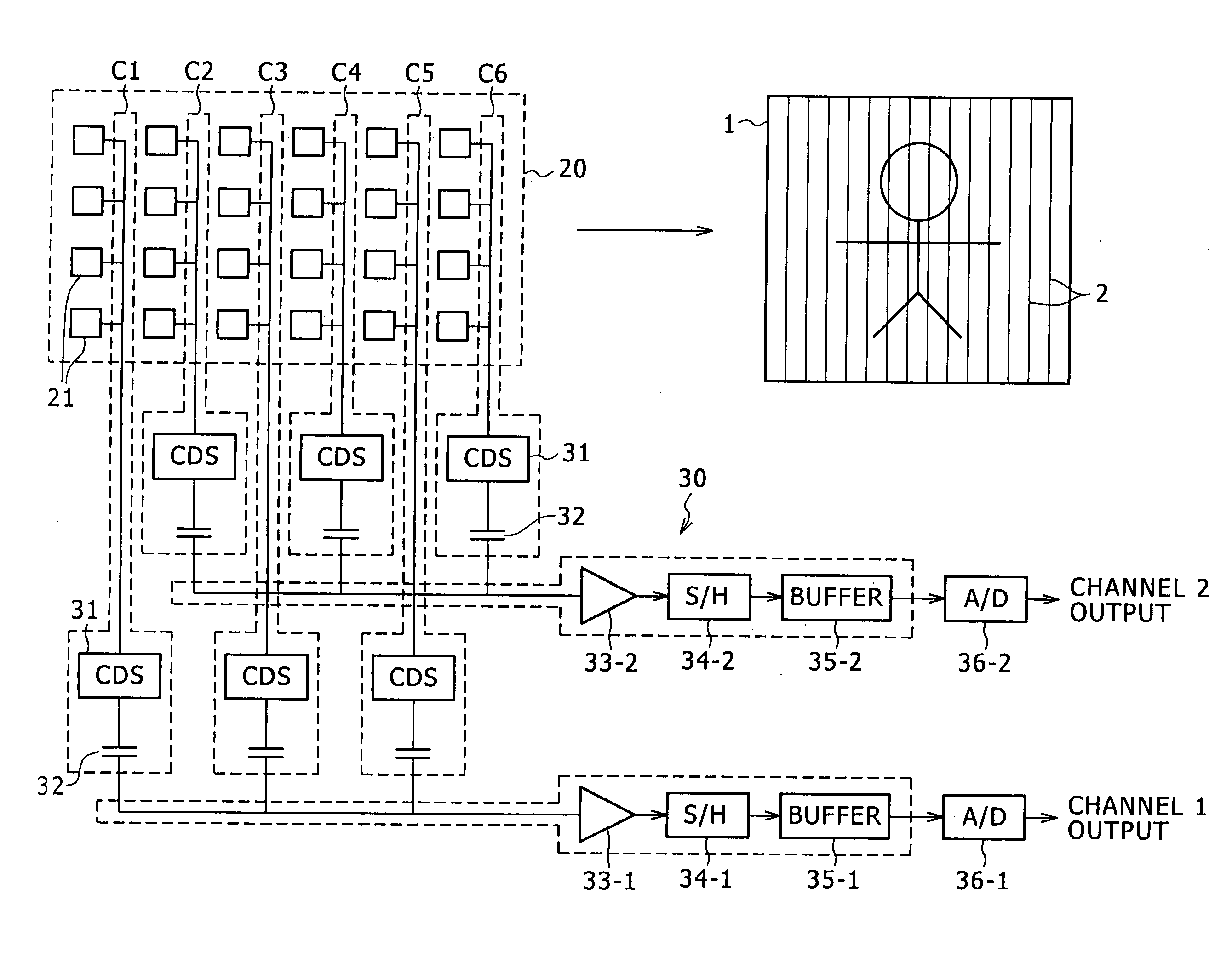
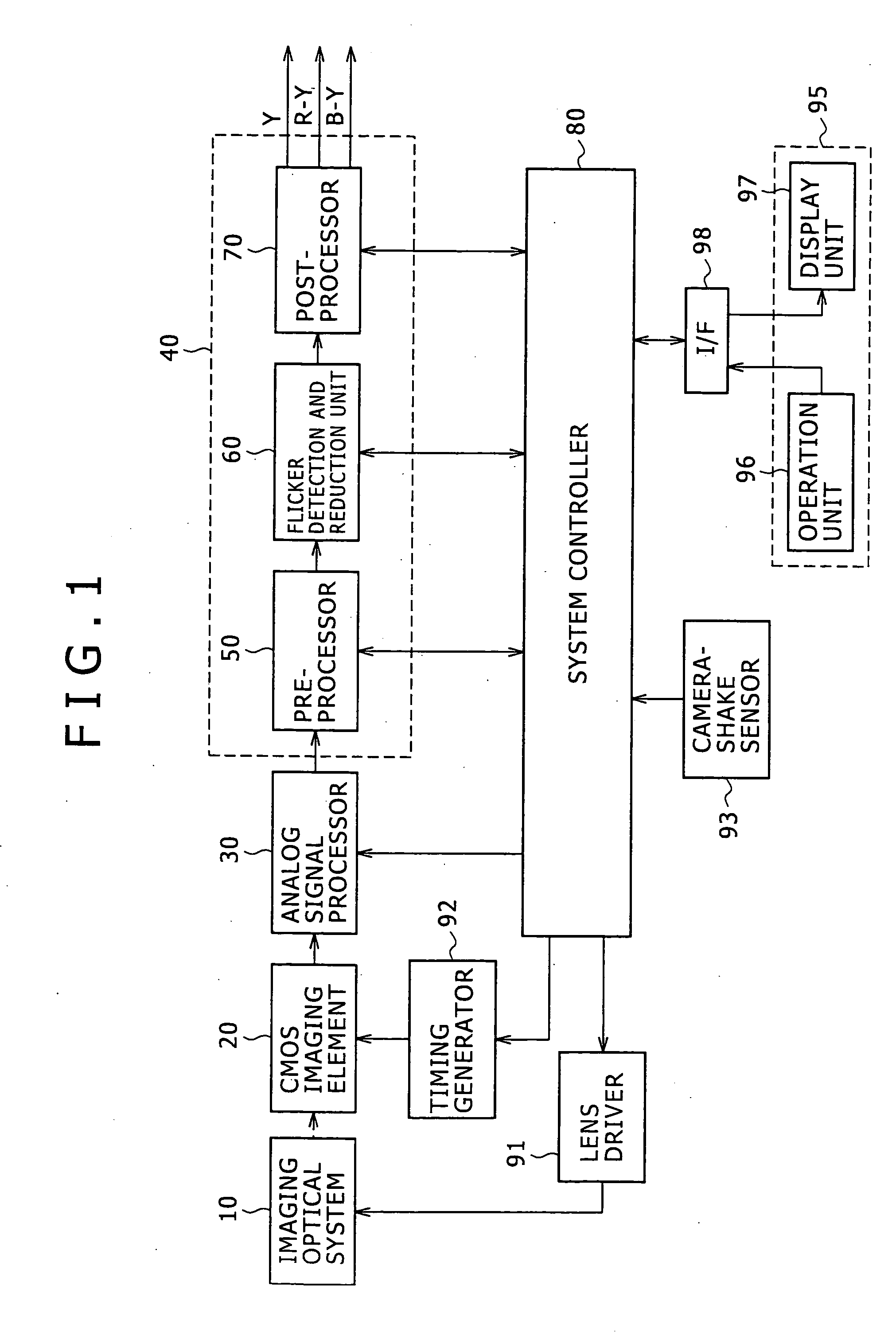
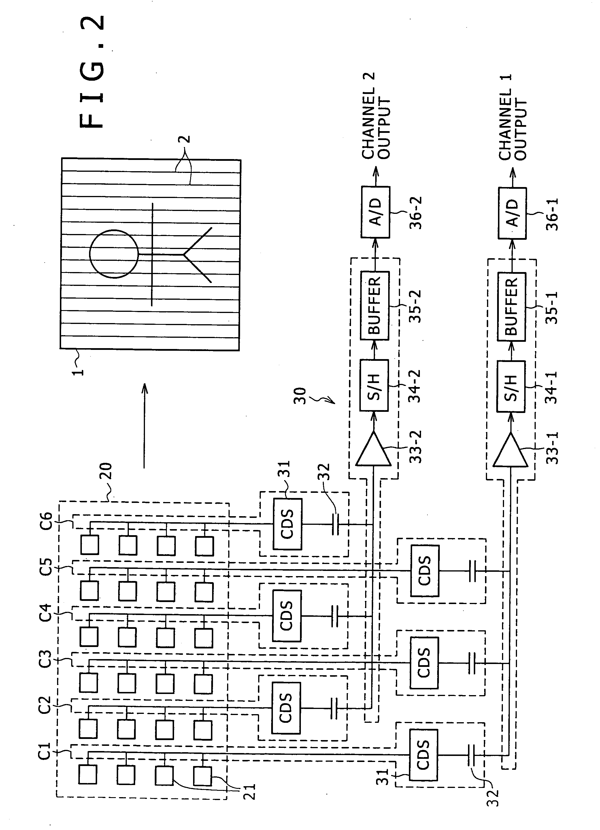
[0045]FIG. 1 illustrates the system configuration of one example of an imaging device according to the present invention, and shows e.g. an NTSC (vertical synchronous frequency is 60 Hz) or PAL (it is 50 Hz) video camera employing a CMOS imaging element as an XY-address scanning-type imaging element.

[0046]In the imaging device of this example, light from an imaging target enters a CMOS imaging element 20 via an imaging optical system 10, followed by being subjected to photoelectric conversion by the CMOS imaging element 20, so that an analog video signal is obtained from the CMOS imaging element 20.

[0047]The CMOS imaging element 20 is formed by two-dimensionally arranging on a CMOS substrate a plurality of pixels each including a photo diode (photo gate), a transfer gate (shutter transistor), a switching transistor (address transistor), an amplifier transistor, a reset transistor (reset gate), and so on. Furthermore, a vertical scan ci...


PUM


Abstract

The present invention is to allow an XY-address scanning-type imaging device such as a CMOS imaging device to detect a fluorescent flicker correctly and accurately and reduce a fluorescent flicker component surely and sufficiently. The RGB primary color signals arising from A/D conversion of the RGB primary color signals obtained from an imaging element are clamped. Subsequently, for the clamped RGB primary color signals, the following processes are executed: correction of the gains of reading-out channels; reduction of fixed pattern noise; correction of the data of defective pixels; noise reduction; lens shading correction; and gain adjustment for exposure adjustment. Thereafter, for the resultant signals, a flicker detection and reduction unit 60 detects and reduces a flicker component. Furthermore, white balance adjustment is implemented for the RGB primary color signals for which the flicker has been reduced, and then defective pixels in the imaging element are detected from the RGB primary color signals for which the white balance adjustment has been executed.

Description

TECHNICAL FIELD[0001]The present invention relates to an imaging device typified by a video camera and a digital still camera employing an XY-address scanning-type imaging element (imager, image sensor) such as a CMOS (complementary metal oxide semiconductor) imaging element, and to a method for processing a video signal obtained from the imaging element when an imaging target is imaged by the imaging device.BACKGROUND ART[0002]When an imaging target is imaged through a video camera under illumination with a fluorescent lamp operated by a commercial AC power supply (home power supply), a video signal as the imaging output involves time-dependent brightness variation, i.e., a so-called fluorescent flicker depending on the difference between the frequency of luminance variation (light amount variation) of the fluorescent lamp (this frequency is twice the power supply frequency) and the vertical synchronous frequency of the camera (imaging frequency).[0003]For example, when an imaging ...

Claims


Application Information

Patent Timeline
IPC IPC(8): H04N9/73H04N5/235H04N5/243H04N5/335H04N5/365H04N5/367H04N5/374H04N101/00
CPCH04N5/2353H04N5/2357H04N5/3572H04N5/3575H04N5/378H04N5/3651H04N5/367H04N5/3742H04N5/361H04N23/745H04N23/73H04N25/616H04N25/61H04N25/671H04N25/68H04N25/63H04N25/767H04N25/75H04N23/70H04N23/76H04N25/60
Inventor KINOSHITA, MASAYA
Owner SONY CORP
Why Eureka
Try Eureka