

High power light emitting diode
- Summary
- Abstract
- Description
- Claims
- Application Information
AI Technical Summary
Benefits of technology
Problems solved by technology
Method used
Image

Examples
Embodiment Construction
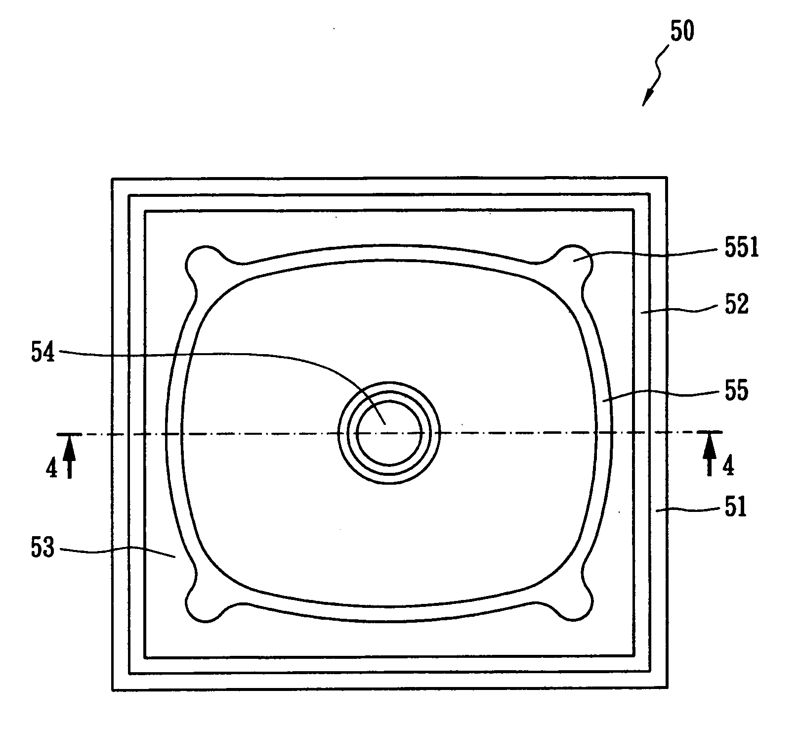
[0036]FIG. 5 and FIG. 6 are respectively the top view and cross-sectional view of a conventional LED 10, wherein FIG. 6 is along line 4-4 in FIG. 5. A high power LED 50 comprises a substrate 57. An N-type semiconductor layer 51, an active layer 56, a P-type semiconductor layer 52 and a transparent conductive layer 53 are sequentially deposited on the substrate 57. A semi-insulator layer or a non-N-type semiconductor layer can be interposed between the N-type semiconductor layer 51 and substrate 57. A N-type electrode 54 with a centralized shape is connected to the under N-type semiconductor layer 51 through an opening 59. The N-type electrode with a centralized pattern is formed on the middle of the LED. As shown in FIG. 1, the round-shaped N-type electrode 54 is placed on the middle of the LED 50. A P-type electrode 55 coupled to the P-type semiconductor layer 52 is arranged like a closed ring or an open ring surrounding the N-type electrode 54, and is stacked on the transparent co...
PUM
 Abstract
Description
Claims
Application Information