Thin film transistor array panel and liquid crystal display

a transistor array and thin film technology, applied in the field of thin film transistor array panels and liquid crystal displays, can solve the problem that the number of gate driving chips does not have a significant effect on manufacturing costs, and achieve the effect of reducing manufacturing costs and reducing the number of driver ic chips

Inactive Publication Date: 2007-04-19
SAMSUNG ELECTRONICS CO LTD
View PDF8 Cites 25 Cited by
  • Summary
  • Abstract
  • Description
  • Claims
  • Application Information

AI Technical Summary

Benefits of technology

[0006] In order to decrease the number of driver IC chips and thus to reduce manufacturing costs it is particularly important to reduce the number of data driver IC chips since they are more expensive than gate driving circuit chip.

Problems solved by technology

While the number of gate lines is doubled, since gate driving chips are inexpensive, the increased number of gate driving chips does not have a significant effect on manufacturing cost.

Method used


Image

  • Thin film transistor array panel and liquid crystal display
  • Thin film transistor array panel and liquid crystal display
  • Thin film transistor array panel and liquid crystal display

Examples


Embodiment Construction

[0027] The present invention will be described more fully hereinafter with reference to the accompanying drawings, in which preferred embodiments of the invention are shown. In the drawings, the thickness of layers, films, panels, regions, etc., are exaggerated for clarity. Like reference numerals designate like elements throughout the specification. It will be understood that when an element such as a layer, film, region, or substrate is referred to as being “on” another element, it can be directly on the other element or intervening elements may also be present. In contrast, when an element is referred to as being “directly on” another element, there are no intervening elements present.

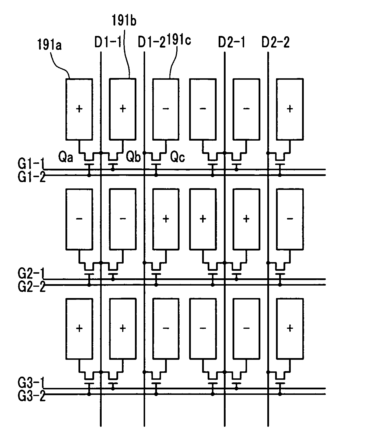
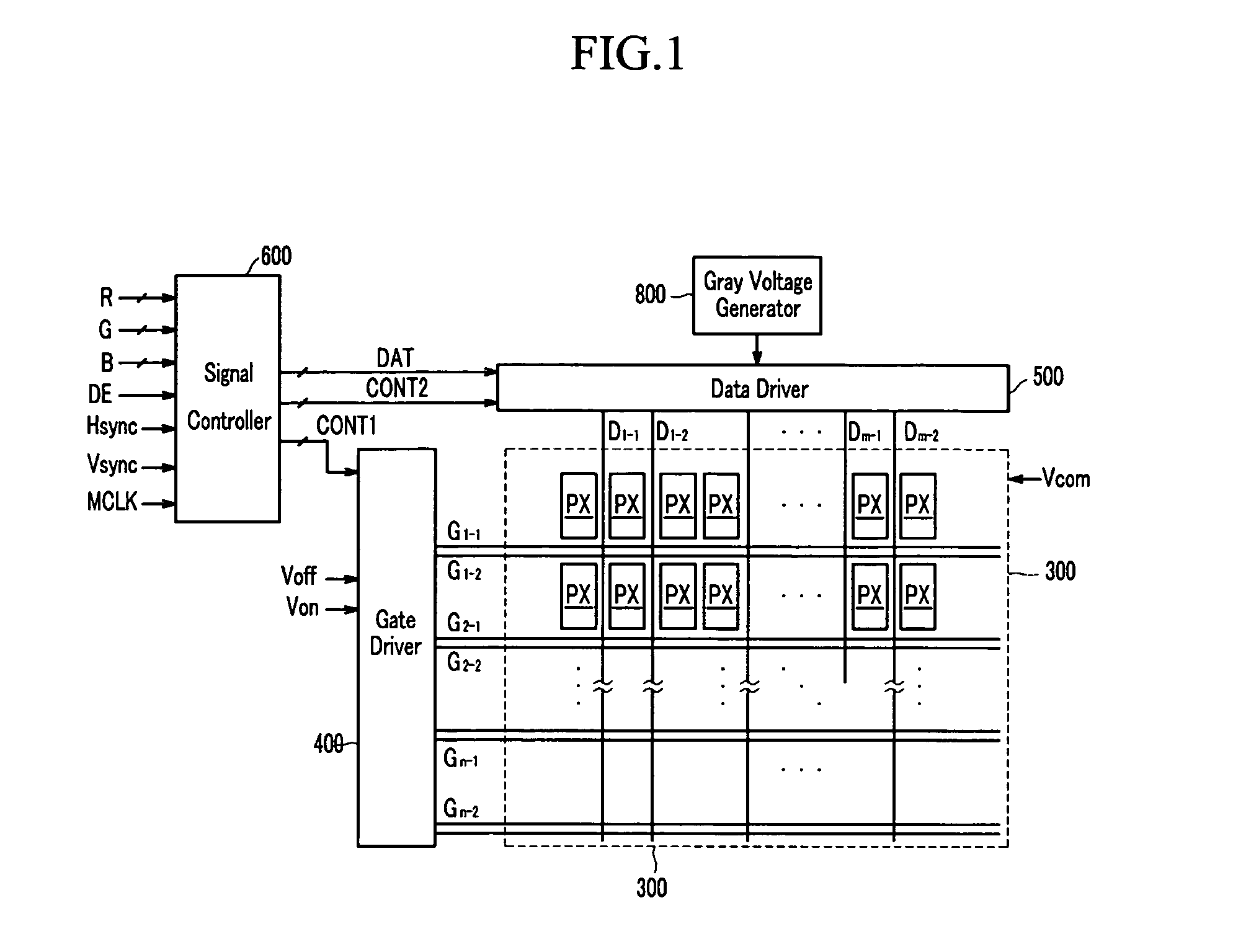
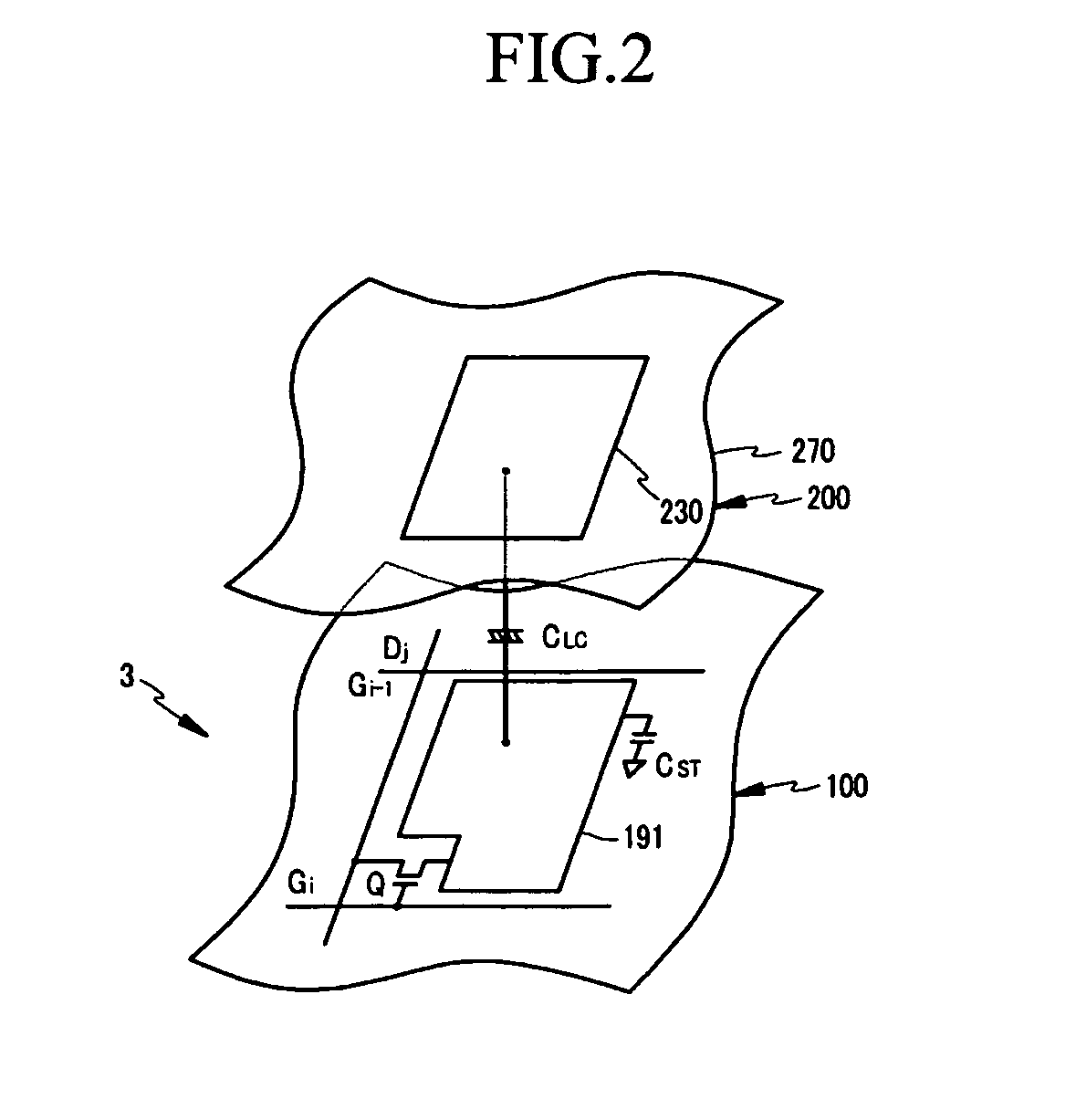
[0028] As shown in FIG. 1, liquid crystal display according to the exemplary embodiment of the present invention includes a liquid crystal panel assembly 300, a gate driver 400 and a data driver 500 connected to liquid crystal panel assembly 300, a gray voltage generator 800 connected to data drive...


PUM


Abstract

A thin film transistor array panel includes: a plurality of pixels including pixel electrodes arranged in a matrix and switching elements connected to the pixel electrodes; first and second gate lines that are connected to the switching elements extend in a row direction and correspond to one row of pixel electrodes; and first and second data lines that are connected to the switching elements extend in a column direction and correspond to three pixel columns. In the thin film transistor array panel, when the three pixel columns are referred to as first to third pixel columns, the pixel electrodes in the first and second pixel columns are connected to the first data line through the switching elements, and the pixel electrodes in the third pixel column are connected to the second data line through the switching elements.

Description

CROSS-REFERENCE TO RELATED APPLICATION [0001] This application claims priority to and the benefit of Korean Patent Application No. 10-2005-0097704 filed in the Korean Intellectual Property Office on Oct. 17, 2005, the entire contents of which are incorporated herein by reference. FIELD OF THE INVENTION [0002] The present invention relates to a liquid crystal display (LCD) having a thin film transistor array panel. DESCRIPTION OF THE RELATED ART [0003] Liquid crystal displays include two display panels, one having pixel electrodes and the other having a common electrode with a liquid crystal layer having dielectric anisotropy between them. Pixel electrodes are arranged in a matrix, and are connected to switching elements such as thin film transistors (TFTs). A data voltage is sequentially applied to the rows of pixel electrodes. Common electrode is supplied with a common voltage. Pixel electrode, common electrode, and the anisotropic dielectric liquid crystal layer form a liquid crys...

Claims


Application Information

Patent Timeline
Patent Type & Authority Applications(United States)
IPC IPC(8): G09G3/36
CPCG02F1/136286G09G3/3607G09G3/3614G09G3/3659G09G2310/0205G02F1/1343
Inventor KIM, DONG-GYU
Owner SAMSUNG ELECTRONICS CO LTD
Why Eureka
Try Eureka