Formation of raised source/drain structures in NFET with embedded SiGe in PFET

a technology of raised source/drain structure and embedded sige, which is applied in the field of semiconductor device fabrication, can solve the problems of complex process and extremely difficult integration of esige in the pfet, and achieve the effect of stable and low resistivity

Active Publication Date: 2007-06-21
TAIWAN SEMICON MFG CO LTD +1
View PDF14 Cites 116 Cited by
  • Summary
  • Abstract
  • Description
  • Claims
  • Application Information

AI Technical Summary

Benefits of technology

[0015] In another aspect, silicide regions are formed and a stressor layer is formed over the structures. The epitaxial Si layer over the PFET embedded Source / drain stressor helps to form stable and low resistivity suicides over the PFET embedded Source / drain stressor.

Problems solved by technology

However, both techniques involve complicated processes compared to a normal CMOS process flow.
It is also extremely difficult to integrate eSiGe in the PFET while having raised S / D structures in the NFET.

Method used


Image

  • Formation of raised source/drain structures in NFET with embedded SiGe in PFET
  • Formation of raised source/drain structures in NFET with embedded SiGe in PFET
  • Formation of raised source/drain structures in NFET with embedded SiGe in PFET

Examples


Embodiment Construction

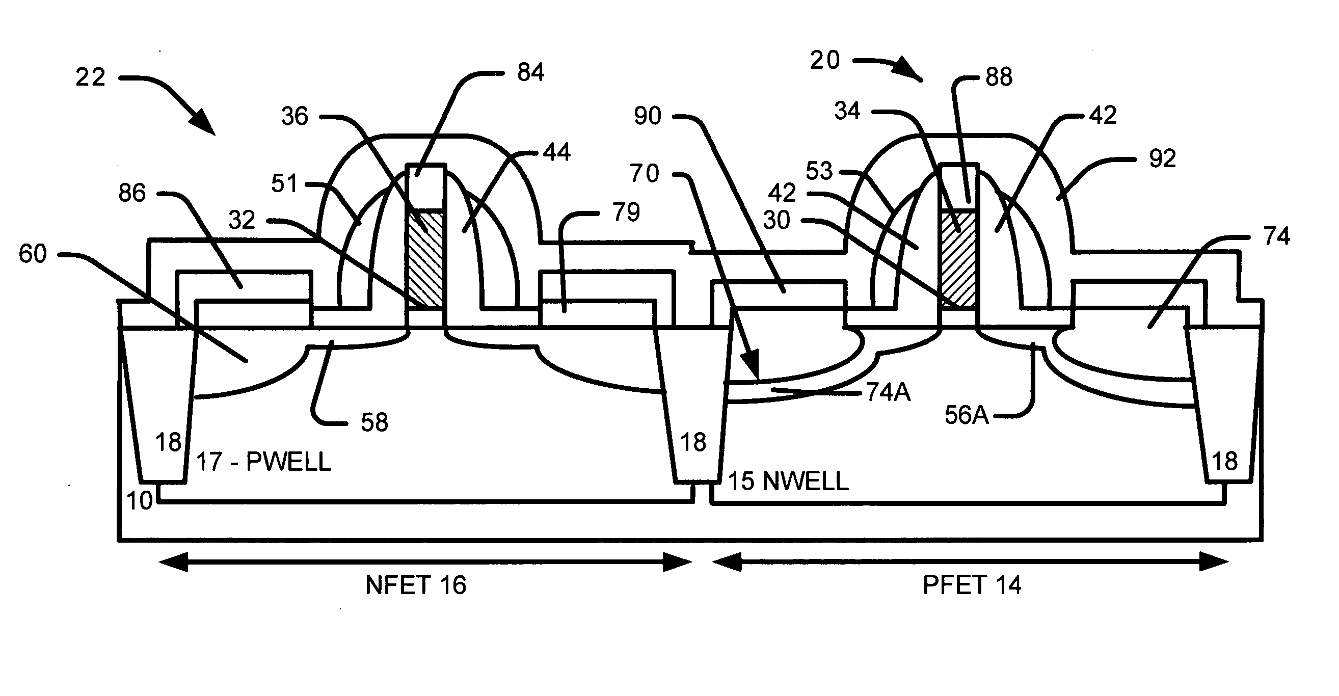
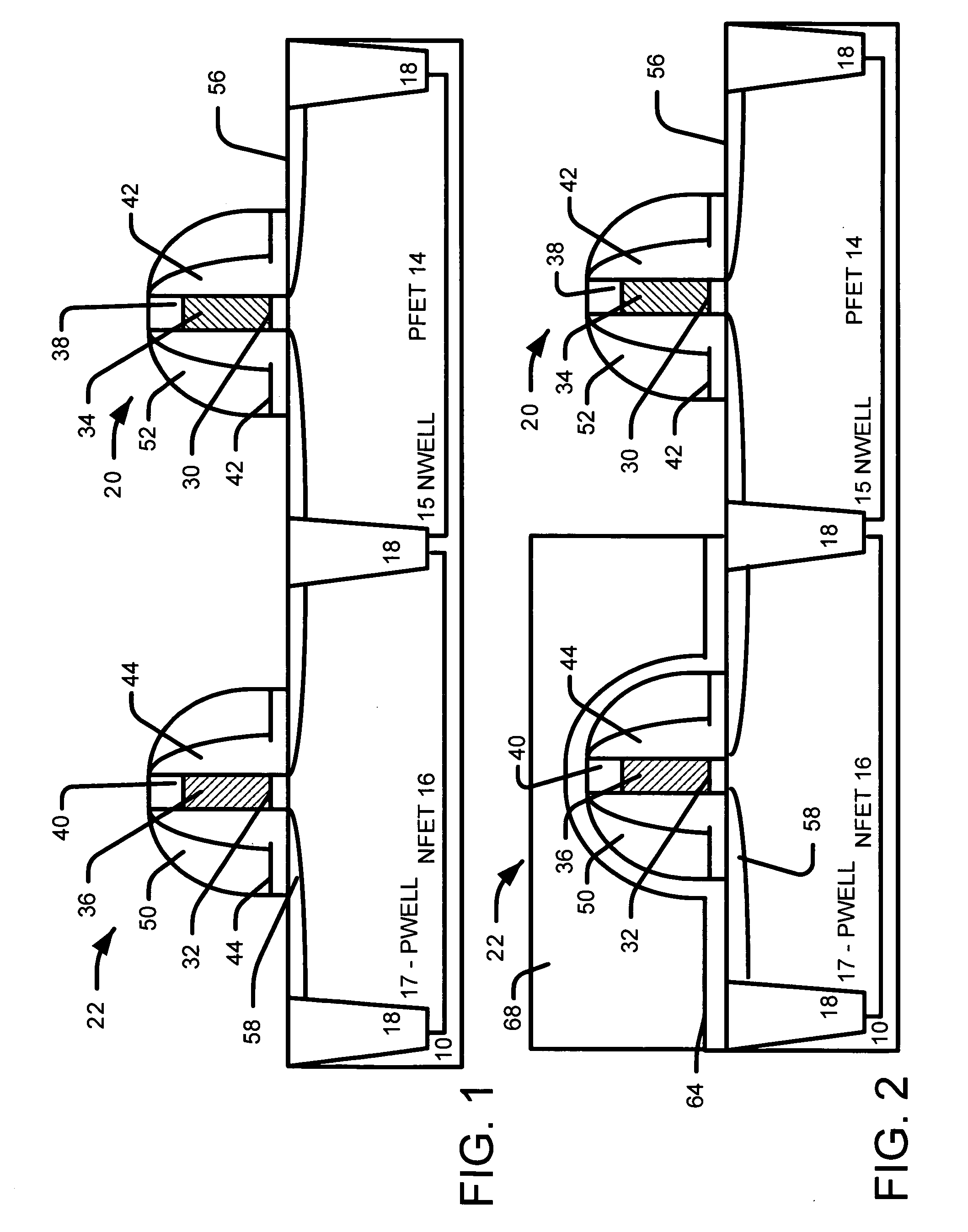
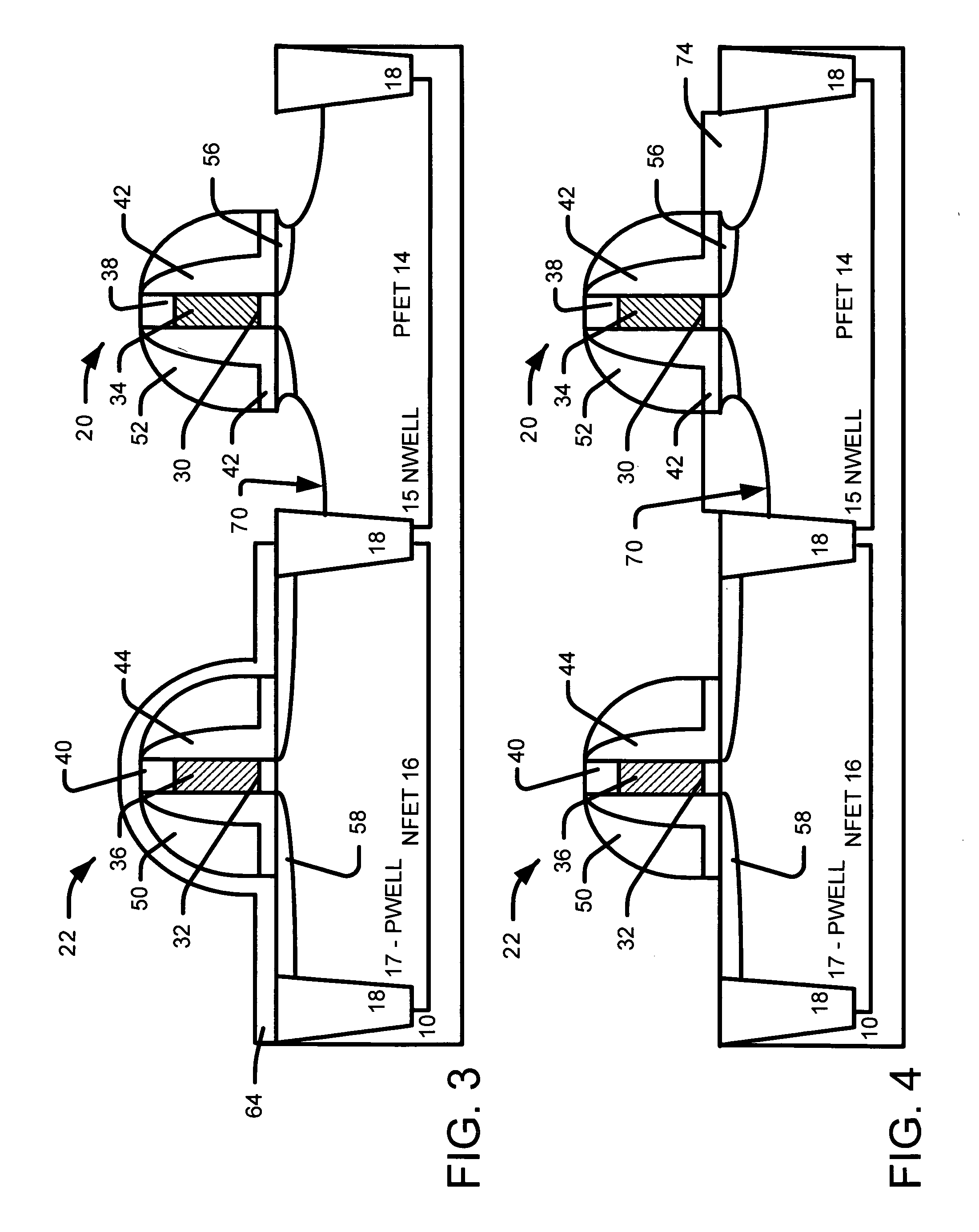
[0021] The example embodiments of the present invention will be described in detail with reference to the accompanying drawings. The example embodiments provide a method of forming a PFET with embedded S / D stressor regions, and raised S / Ds in the NFET. In addition, a stress liner can be formed over reduced spacers of the FET gate.

A. Provide a NFET Gate Structure Over a NFET Region in a Substrate and PFET Gate Structure Over a PFET Region

[0022] Referring to FIG. 1, we provide a NFET gate structure 22 over a NFET region 16 in a substrate 10 and PFET gate structure 20 over a PFET region 14.

[0023] The NFET gate structure 22 is comprised of a NFET gate dielectric 32, a NFET gate 36, NFET gate cap layer 40 over the NFET gate 36, NFET first (L-shaped) spacers 44, and NFET second spacers 50. The gate cap layer 40 can be comprised of silicon nitride. The NFET second spacers 50 can be comprised of silicon nitride.

[0024] The PFET gate structure 20 is preferably comprised of a PFET gate di...


PUM


Abstract

A structure and method for forming raised source/drain structures in a NFET device and embedded SiGe source/drains in a PFET device. We provide a NFET gate structure over a NFET region in a substrate and PFET gate structure over a PFET region. We provide NFET SDE regions adjacent to the NFET gate and provide PFET SDE regions adjacent to the PFET gate. We form recesses in the PFET region in the substrate adjacent to the PFET second spacers. We form a PFET embedded source/drain stressor in the recesses. We form a NFET S/D epitaxial Si layer over the NFET SDE regions and a PFET S/D epitaxial Si layer over PFET embedded source/drain stressor. The epitaxial Si layer over PFET embedded source/drain stressor is consumed in a subsequent salicide step to form a stable and low resistivity silicide over the PFET embedded source/drain stressor. We perform a NFET S/D implant by implanting N-type ions into NFET region adjacent to the NFET gate structure and into the NFET S/D stressor Si layer to form the raised NFET source/drains.

Description

BACKGROUND OF INVENTION [0001] 1) Field of the Invention [0002] This invention relates generally to devices and methods for the fabrication of semiconductor devices and more particularly to the fabrication of Field Effect Transistors (FETs) having embedded Source / Drain regions and FETs having raised S / D regions. [0003] 2) Description of the Prior Art [0004] It is now well-established that raised source / drain (S / D) structures and embedded SiGe (eSiGe) are useful techniques to enhance device performance. However, both techniques involve complicated processes compared to a normal CMOS process flow. Especially for eSiGe, besides the additional process needed for Si recess and epitaxial growth in the PFET S / D region, the eSiGe scheme needs additional process to protect the poly-Si gate as well. It is also extremely difficult to integrate eSiGe in the PFET while having raised S / D structures in the NFET. [0005] The importance of overcoming the various deficiencies noted above is evidenced ...

Claims


Application Information

Patent Timeline
Patent Type & Authority Applications(United States)
IPC IPC(8): H01L29/76H01L21/8238
CPCH01L21/823807H01L21/823814H01L21/823864H01L29/66545H01L29/6656H01L29/66628H01L29/66636H01L29/7848
Inventor CHONG, YUNG FULUO, ZHIJIONGKIM, JOO CHANHOLT, JUDSON ROBERT
Owner TAIWAN SEMICON MFG CO LTD
Why Eureka
Try Eureka