Substrate for forming passive elements in chip type

a passive element and substrate technology, applied in the field of substrates, can solve the problems of adversely affecting yield and the conductivity of inner electrodes

Inactive Publication Date: 2007-08-23
WALSIN TECHNOLOGY CORPORATION
View PDF6 Cites 2 Cited by
  • Summary
  • Abstract
  • Description
  • Claims
  • Application Information

AI Technical Summary

Problems solved by technology

Therefore, conductivity of the inner electrodes (38) will vary and adversely influence yield due to inconsistent thickness of the inner electrodes (38).

Method used


Image

  • Substrate for forming passive elements in chip type
  • Substrate for forming passive elements in chip type
  • Substrate for forming passive elements in chip type

Examples


Embodiment Construction

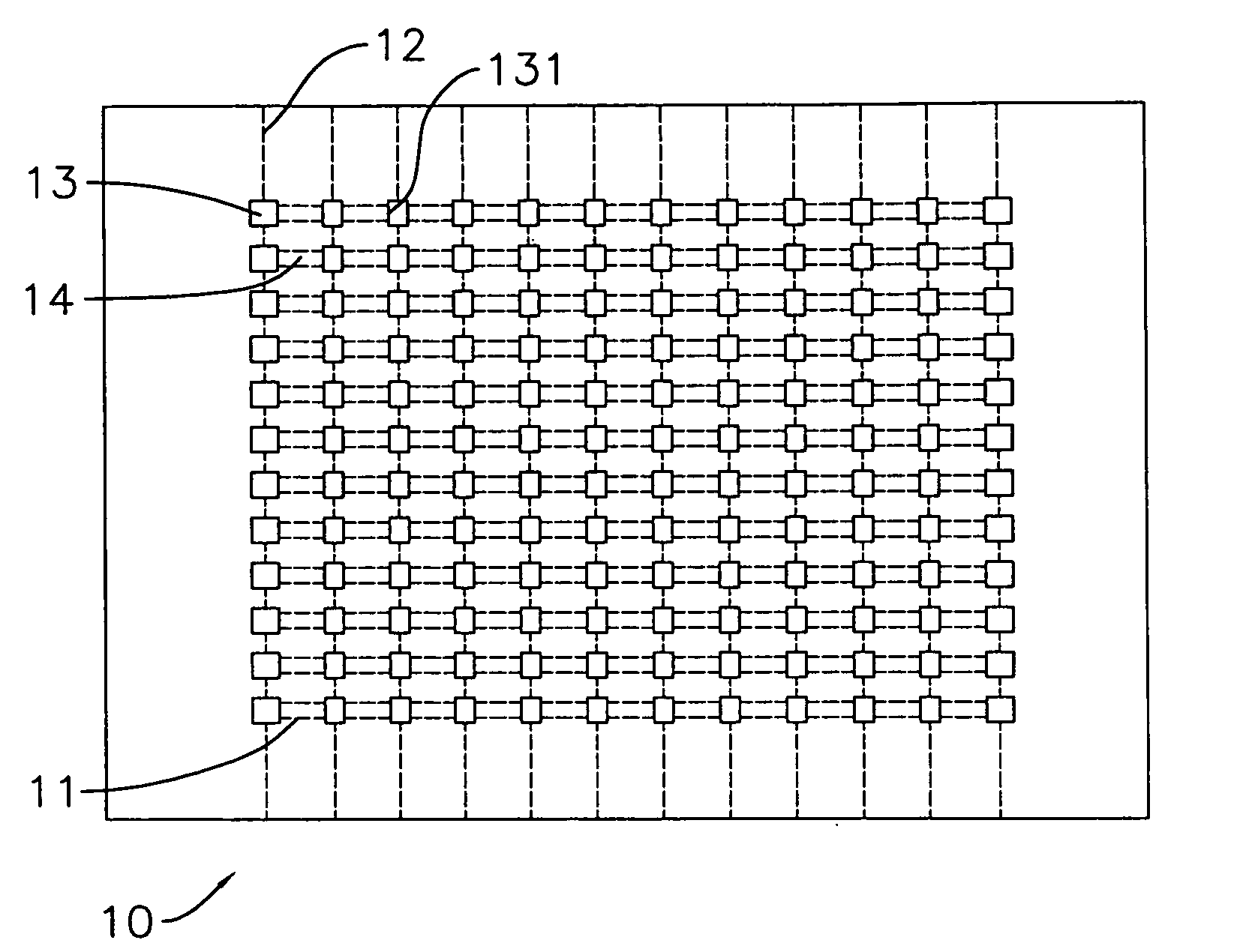
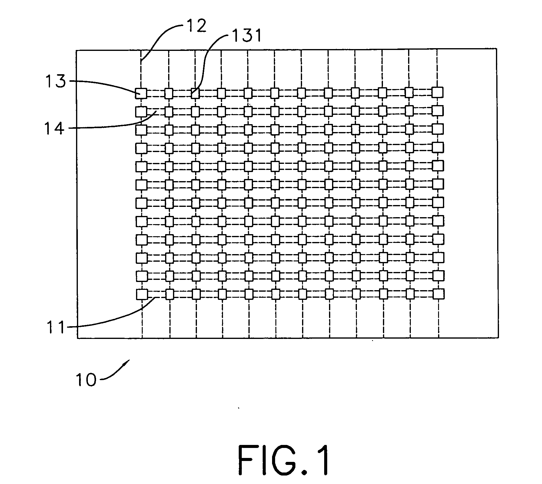
[0026]With reference to FIG. 1, a substrate (10) in accordance with the present invention may be made of cermet, can be used to manufacture chip resistors and has a top surface, a thickness, multiple parallel grooves (11), multiple optional perpendicular grooves (12), multiple through holes (13) and multiple chip regions (14).

[0027]The parallel grooves (11) are formed on the top surface of the substrate (10), may be formed by cutting the substrate (10) with a blade and respectively have a depth. The depth of each parallel groove (11) may not be deeper than half the thickness of the substrate (10).

[0028]The perpendicular grooves (12) are formed across the parallel grooves (11) on the top surface of the substrate (10), may be formed by cutting the substrate (10) with a blade and respectively have a depth. The depth of each perpendicular groove (11) may not be deeper than half the thickness of the substrate (10).

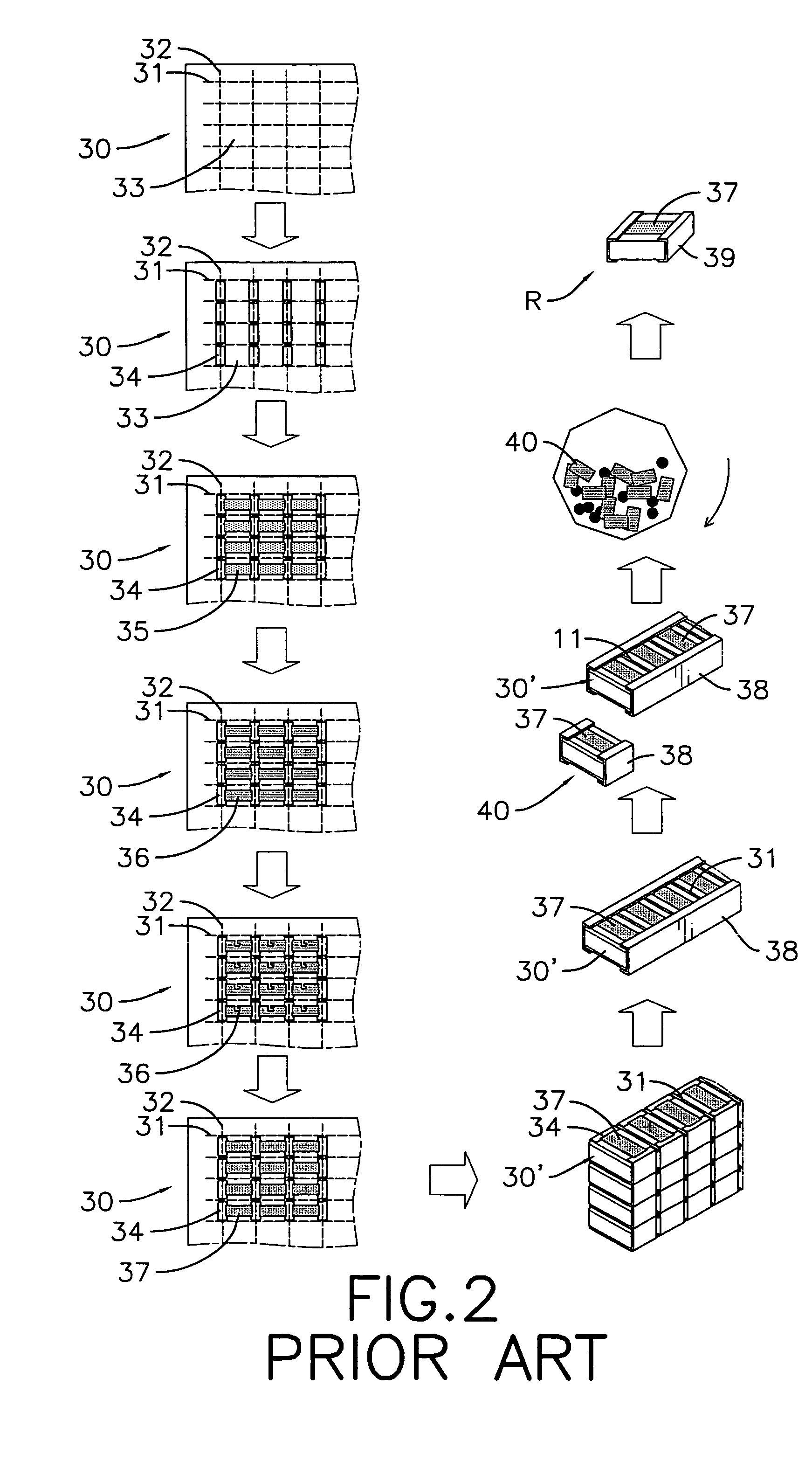
[0029]The through holes (13) are formed between and across two adjacent pa...


PUM


Abstract

A substrate for forming passive elements in chip type has a top surface, a thickness, multiple parallel grooves, multiple through holes and multiple chip regions. The parallel grooves are formed on the top surface of the substrate. The through holes are formed between and across two adjacent parallel grooves, and each through hole is separated from other through holes and has smooth inner walls. The chip regions are defined between adjacent through holes and parallel grooves and are arranged in a matrix.

Description

BACKGROUND OF THE INVENTION[0001]1. Field of the Invention[0002]The present invention relates to a substrate, and more particularly to a substrate for forming passive elements in chip type.[0003]2. Description of Related Art[0004]Because electronic products are becoming smaller, individual active and passive electronic elements have to become smaller, too. For example, standard chip resistors may be 0.60 mm in length, 0.30 mm in width and 0.23 mm in depth or 0.40 mm in length, 0.20 mm in width and 0.23 mm in depth. Smaller elements have smaller tolerances for error.[0005]With reference to FIG. 2, a conventional manufacturing method comprises steps of etching grooves (31, 32) on a substrate (30), defining chip regions (33), forming main electrodes (34), forming resistor layers (35), forming inner protective layers (36), adjusting resistance, forming outer protective layers (37), dividing the substrate (30) into multiple strips (30′), forming inner electrodes (38), cutting the strips ...

Claims


Application Information

Patent Timeline
Patent Type & Authority Applications(United States)
IPC IPC(8): G02B6/30
CPCH01C7/001H01C17/006H01C7/003
Inventor LUH, SHIOW-CHANGKUO, CHUN-HSIUNG
Owner WALSIN TECHNOLOGY CORPORATION
Why Eureka
Try Eureka