

Liquid crystal display device
- Summary
- Abstract
- Description
- Claims
- Application Information
AI Technical Summary
Benefits of technology
Problems solved by technology
Method used
Image

Examples
first embodiment
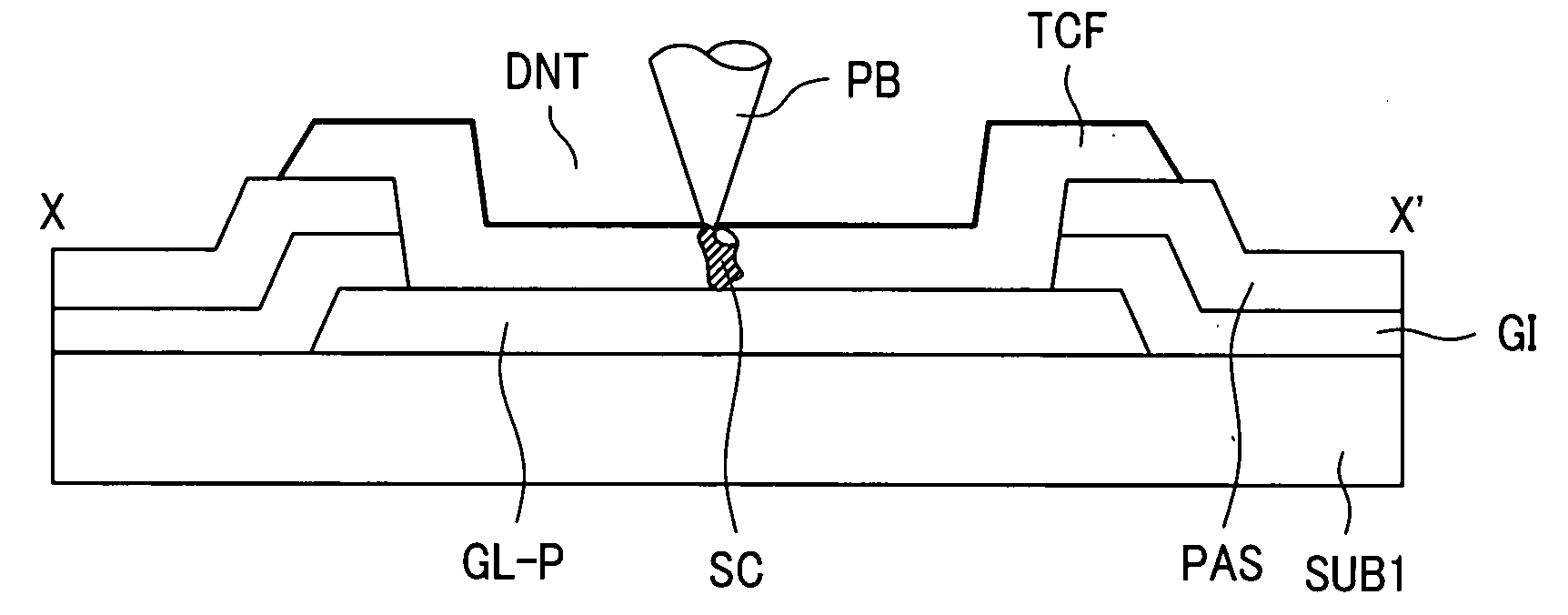
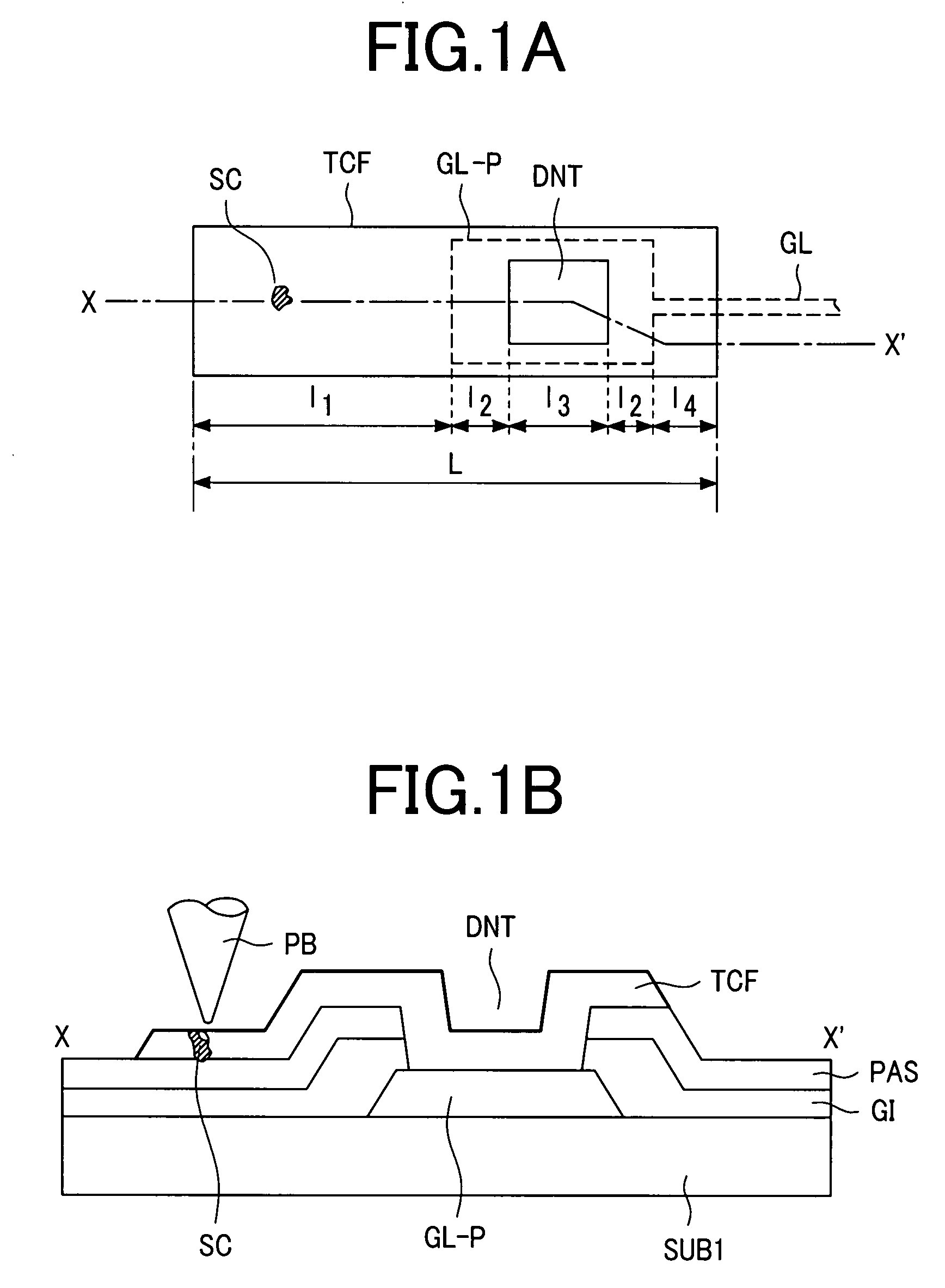
[0029]FIG. 1 is a diagram showing a structure of a wire inspection terminal of a scanning wire and disconnection inspection by the contact of an inspection probe according to a first embodiment of the present invention. Like FIG. 6, FIG. 1 explains disconnection inspection of a scanning wire formed on a thin-film transistor substrate SUB1 which is a first substrate. FIG. 1A is an enlarged view of a portion of a wire inspection terminal GL-P. FIG. 1B is a cross-sectional view taken along the X-X′ line of FIG. 1A. A wire inspection terminal (pad) GL-P is formed at the end of a scanning wire (gate wire) GL on the main surface of the thin-film transistor substrate SUB1 suitably made of a glass plate.
[0030]Like in FIG. 6, an insulating film composed of a gate insulating film GI and a protection film PAS is formed on the gate wire GL and the wire inspection terminal GL-P, i.e., the wide portion. On the upper surface of the wire inspection terminal GL-P, this insulating film is partially r...
second embodiment
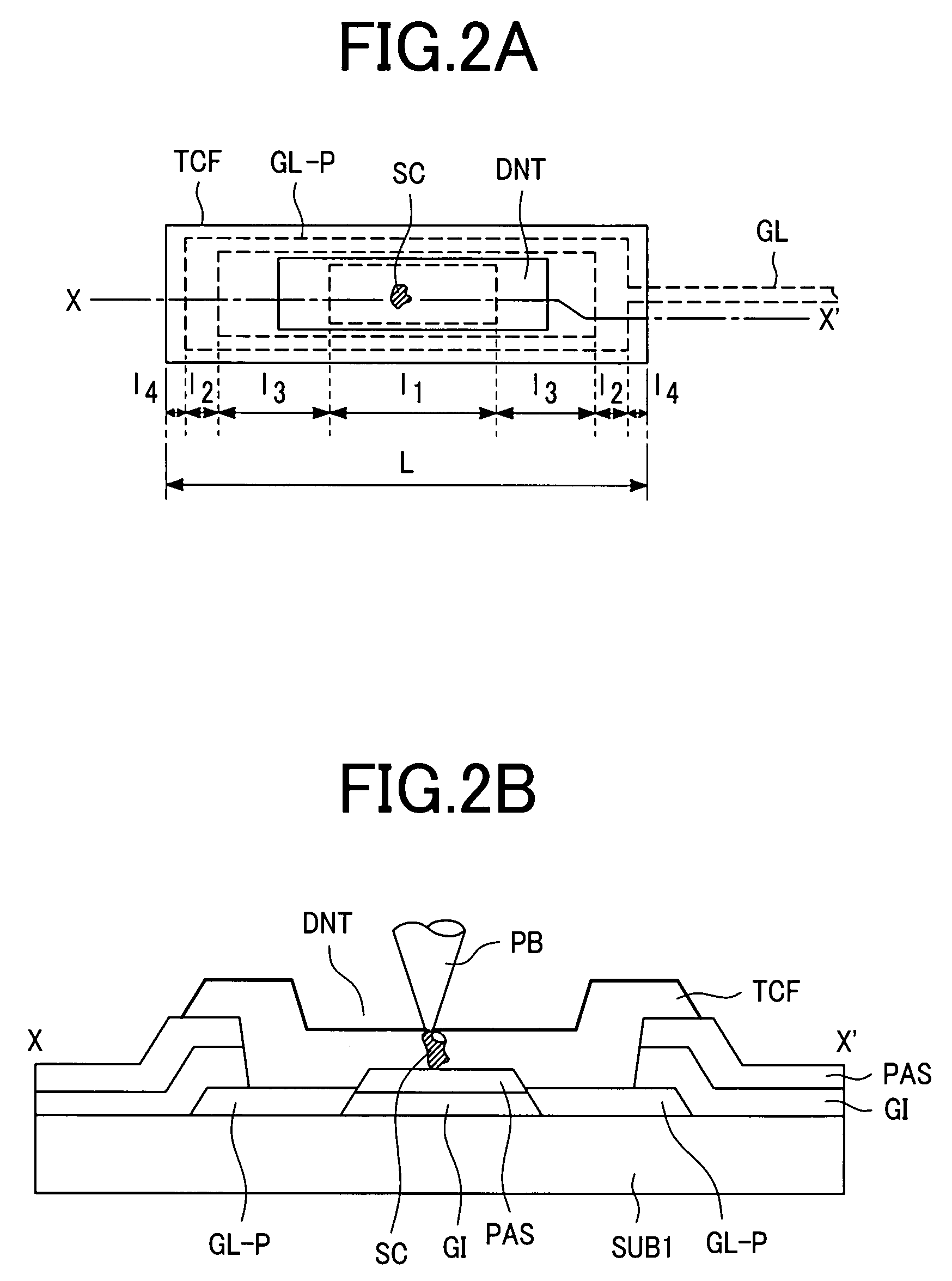
[0034]FIG. 2 is a diagram showing a structure of a wire inspection terminal of a scanning wire and disconnection inspection by the contact of an inspection probe according to a second embodiment of the present invention. Like FIG. 2, FIG. 1 explains disconnection inspection of a scanning wire formed on a thin-film transistor substrate SUB1 which is a first substrate. FIG. 2A is an enlarged view of a portion of a wire inspection terminal GL-P. FIG. 2B is a cross-sectional view taken along the X-X′ line of FIG. 2A. A wire inspection terminal (pad) GL-P is formed at the end of a scanning wire (gate wire) GL on the main surface of the thin-film transistor substrate SUB1 suitably made of a glass plate.
[0035]Like FIG. 1, an insulating film composed of a gate insulating film GI and a protection film PAS is formed on the gate wire GL and the wire inspection terminal GL-P, i.e., the wide portion. Then, this insulating film has been removed at the central part of the wire inspection terminal ...
third embodiment
[0037]FIG. 3 is a diagram showing a structure of a wire inspection terminal of a scanning wire and disconnection inspection by the contact of an inspection probe according to a third embodiment of the present invention. Like FIG. 2, FIG. 3 explains disconnection inspection of a scanning wire formed on a thin-film transistor substrate SUB1 which is a first substrate. FIG. 3A is an enlarged view of a portion of a wire inspection terminal GL-P. FIG. 3B is a cross-sectional view taken along the X-X′ line of FIG. 3A. A wire inspection terminal (pad) GL-P is formed at the end of a scanning wire (gate wire) GL on the main surface of the thin-film transistor substrate SUB1 suitably made of a glass plate.
[0038]Like FIG. 2, an insulating film composed of a gate insulating film GI and a protection film PAS is formed on the gate wire GL and the wire inspection terminal GL-P, i.e., the wide portion. Then, this insulating film has been removed from other than the central part and peripheral part ...
PUM
 Abstract
Description
Claims
Application Information