Self-aligned pillar patterning using multiple spacer masks

a technology of spacer masks and pillars, applied in the field of semiconductor/solid-state device manufacturing, basic electric elements, electric devices, etc., can solve the problems of increasing the difficulty of reducing the critical dimension of the lithographic process used to pattern these building blocks, and the difficulty of reducing the critical dimension at the expense of increasing the spacing between features

Inactive Publication Date: 2009-01-15
APPLIED MATERIALS INC
View PDF6 Cites 350 Cited by
  • Summary
  • Abstract
  • Description
  • Claims
  • Application Information

AI Technical Summary

Problems solved by technology

As the dimensions of the fundamental building blocks of microelectronic circuitry are reduced and as the sheer number of fundamental building blocks fabricated in a given region is increased, the constraints on the lithographic processes used to pattern these building blocks have become overwhelming.
However, this reduction in critical dimension comes at the expense of an increased spacing between features, as depicted by spacing ‘y’ in FIG. 1C.

Method used


Image

  • Self-aligned pillar patterning using multiple spacer masks
  • Self-aligned pillar patterning using multiple spacer masks
  • Self-aligned pillar patterning using multiple spacer masks

Examples


Embodiment Construction

[0015]A method of self-aligned pillar patterning using multiple spacer masks is described. In the following description, numerous specific details are set forth, such as fabrication conditions and material regimes, in order to provide a thorough understanding of the present invention. It will be apparent to one skilled in the art that the present invention may be practiced without these specific details. In other instances, well-known features, such as integrated circuit design layouts or photoresist development processes, are not described in detail in order to not unnecessarily obscure the present invention. Furthermore, it is to be understood that the various embodiments shown in the FIGS. are illustrative representations and are not necessarily drawn to scale.

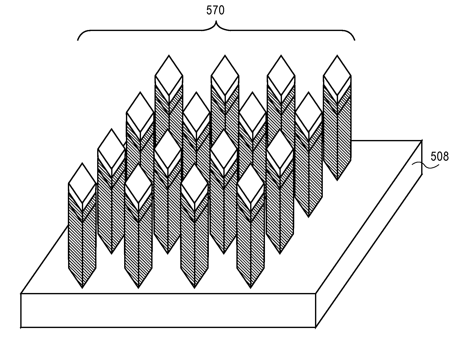
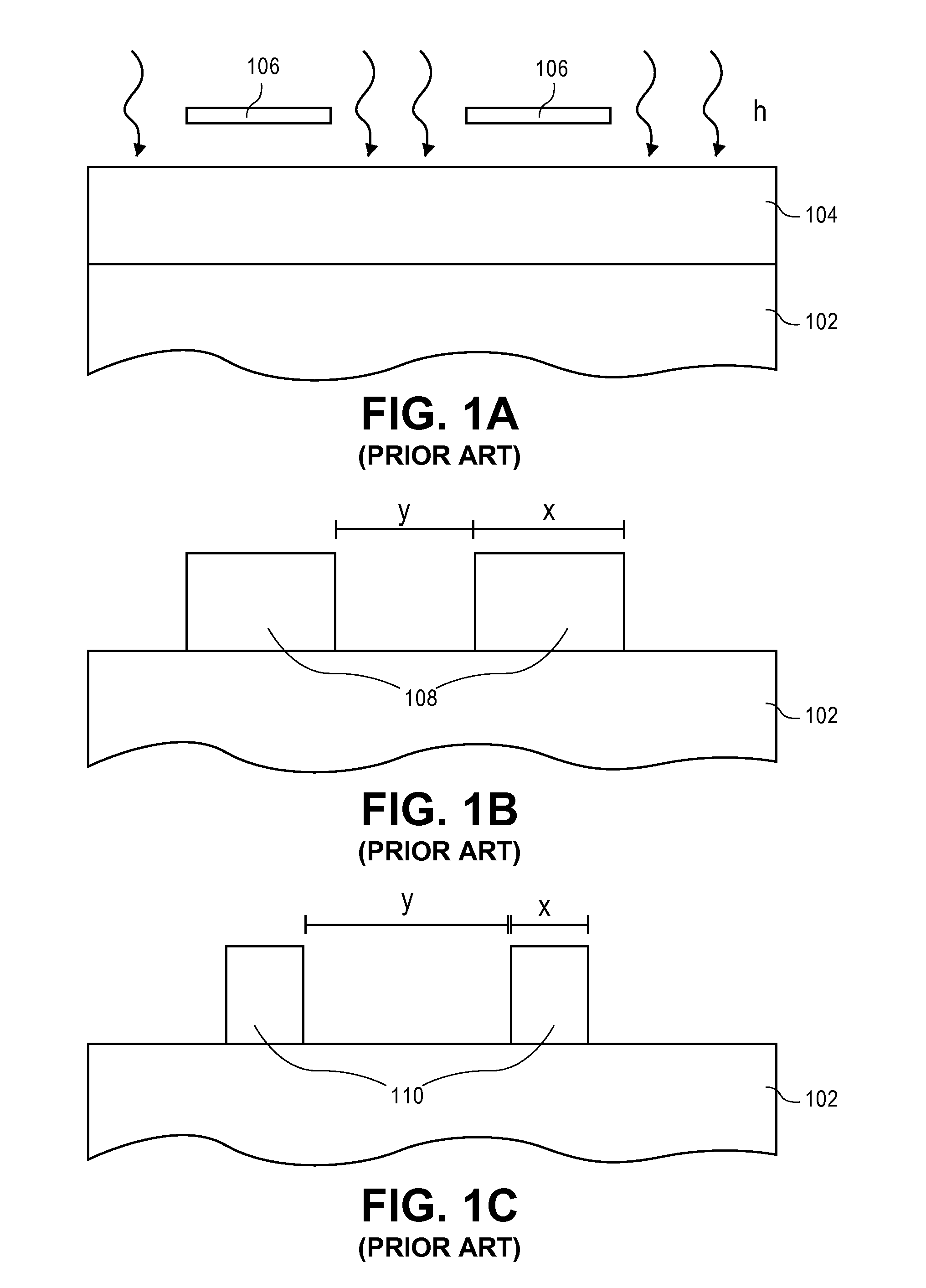
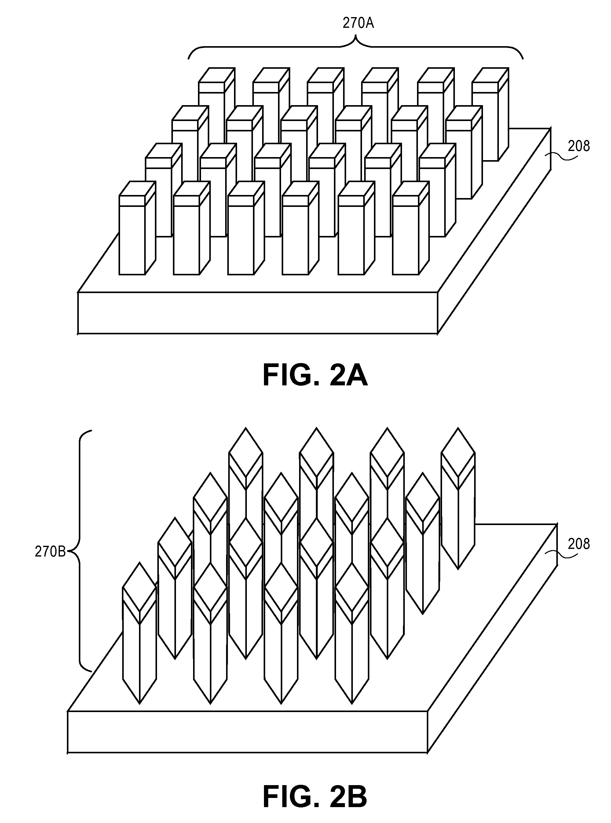
[0016]Disclosed herein is a method for fabricating a semiconductor mask. The image of a series of lines from a first spacer mask may first be provided to a mask layer to form a patterned mask layer. In an embodiment, the im...


PUM


Abstract

A method for fabricating a semiconductor mask is described. The image of a series of lines from a first spacer mask is first provided to a mask layer to form a patterned mask layer. The image of a series of lines from a second spacer mask is then provided to the patterned mask layer to form a pillar mask comprised of a series of pillars. The image of the series of lines from the second spacer mask is non-parallel with the series of lines from the first spacer mask.

Description

CROSS REFERENCE TO RELATED APPLICATIONS[0001]This application claims the benefit of U.S. Provisional Application No. 60 / 932,635 filed Jun. 1, 2007, the entire contents of which are hereby incorporated by reference herein.BACKGROUND OF THE INVENTION[0002]1) Field of the Invention[0003]The invention is in the field of Semiconductor Processing.[0004]2) Description of Related Art[0005]For the past several decades, the scaling of features in integrated circuits has been the driving force behind an ever-growing semiconductor industry. Scaling to smaller and smaller features enables increased densities of functional units on the limited real estate of semiconductor chips. For example, shrinking transistor size allows for the incorporation of an increased number of logic and memory devices on a microprocessor, lending to the fabrication of products with increased complexity.[0006]Scaling has not been without consequence, however. As the dimensions of the fundamental building blocks of micro...

Claims


Application Information

Patent Timeline
Patent Type & Authority Applications(United States)
IPC IPC(8): H01L21/311
CPCH01L21/0338H01L21/0334
Inventor BENCHER, CHRISTOPHER D.
Owner APPLIED MATERIALS INC
Why Eureka
Try Eureka