Substrate structure and electronic apparatus

Inactive Publication Date: 2009-02-05
PANASONIC CORP
View PDF9 Cites 3 Cited by
  • Summary
  • Abstract
  • Description
  • Claims
  • Application Information

AI Technical Summary

Benefits of technology

[0042]According to the invention, it has an effect capable of miniaturizing and thinning a circuit substrate or an electronic apparatus using the circuit substrate by receiving an electronic component in a through hole.
[0043]Further, according to the invention, it has an effect capable of preventing the electronic component from touching a resin part by covering the through hole with a lid member.

Problems solved by technology

However, when an electronic component 106 is mounted on the soft wiring 105 of the display device 103, a thickness dimension of the whole substrate structure increases by the amount of a height dimension H of the electronic component 106 and it becomes an obstacle to thinning and miniaturization of the portable terminal.

Method used


Image

  • Substrate structure and electronic apparatus
  • Substrate structure and electronic apparatus
  • Substrate structure and electronic apparatus

Examples


first embodiment

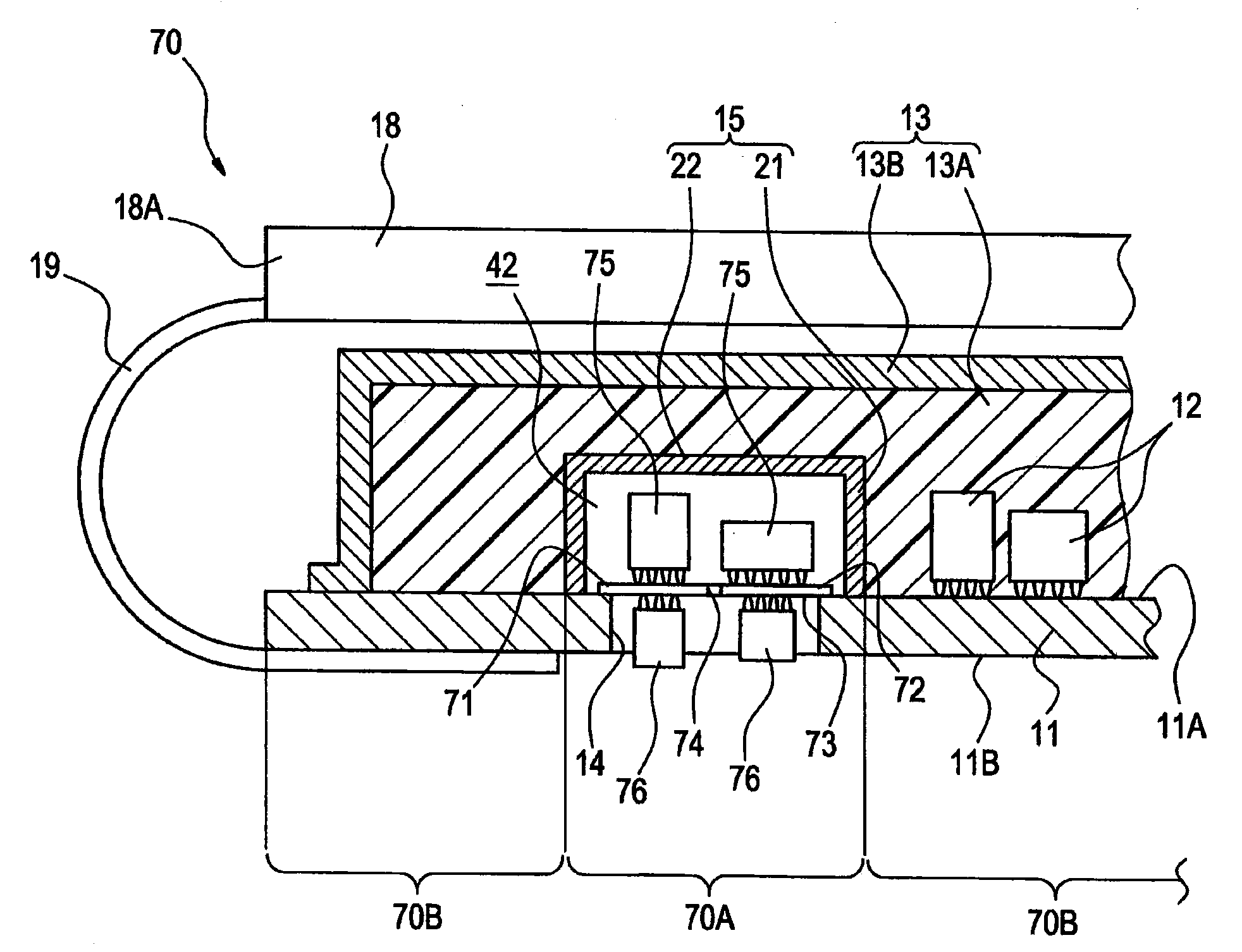
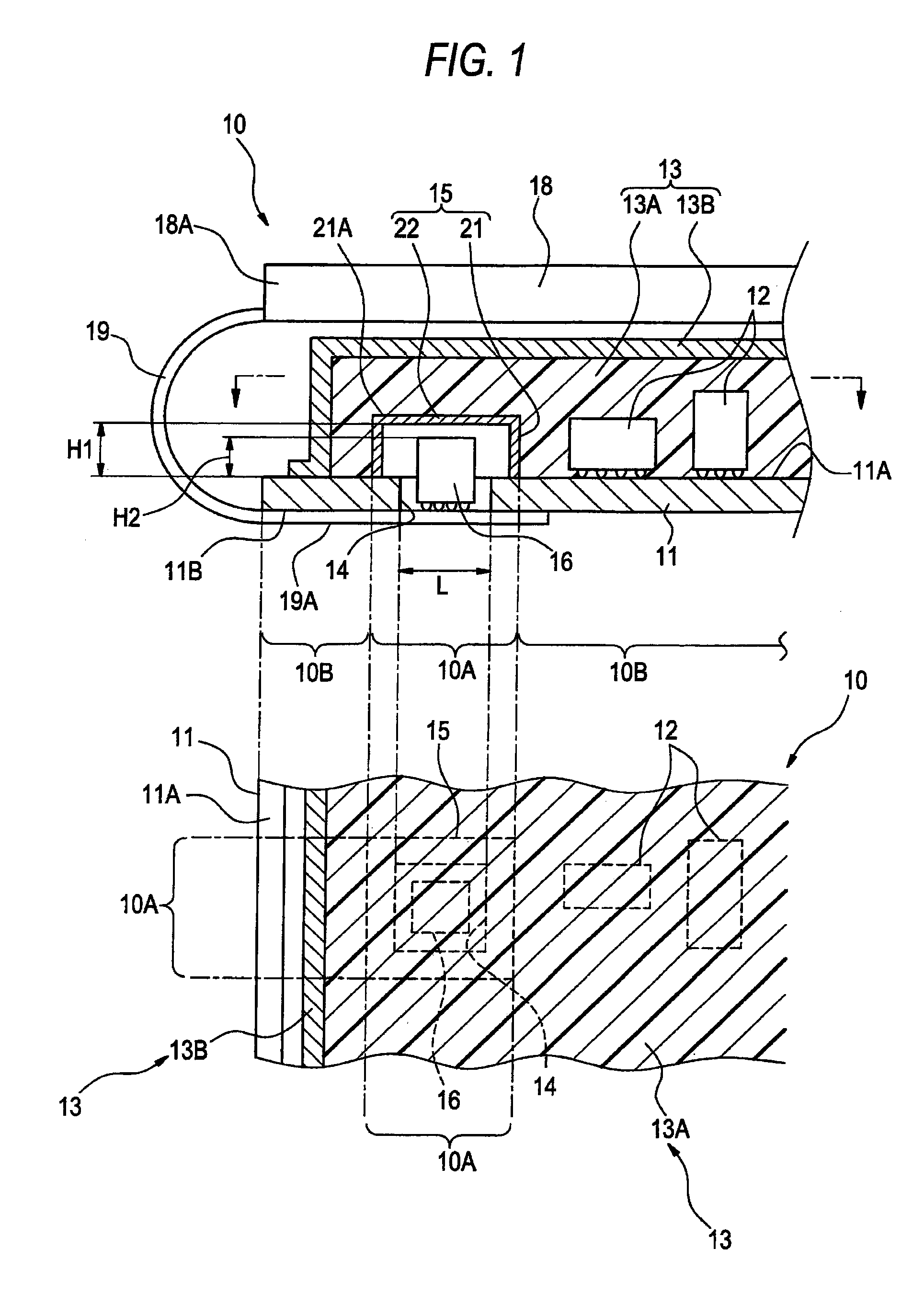
[0066](First Embodiment)

[0067]As shown in FIG. 1, a substrate structure 10 of a first embodiment comprises a substrate 11, plural electronic components 12 mounted along one mounting surface 11A on the substrate 11, and a resin part 13 for making close contact with the mounting surface 11A of the substrate 11 while each of the electronic components 12 is covered with a resin 13A, and is received in a housing of an electronic apparatus such as a portable terminal.

[0068]In this substrate structure 10, a through hole 14 is disposed in the substrate 11 and also the side of the mounting surface 11A in the through hole 14 is closed by a lid member 15 and an electronic component 16 is received in the through hole 14.

[0069]In this substrate 11, a support member (not shown) is disposed so as to stride over the resin part 13, and a display device 18 such as an LCD is supported in this support member. Soft wiring 19 is led from an end face 18A of the display device 18, and the end 19A of the so...

second embodiment

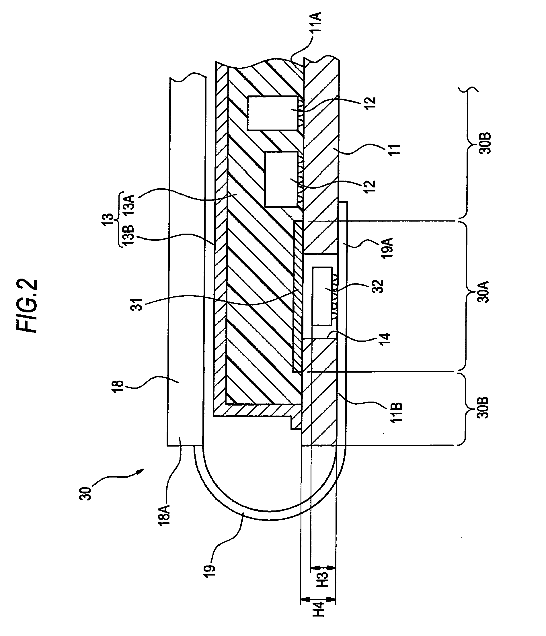
[0093](Second Embodiment)

[0094]As shown in FIG. 2, a substrate structure 30 of a second embodiment is a structure using a lid member 31 instead of the lid member 15 of the first embodiment, and the other configuration is similar to that of the first embodiment.

[0095]The lid member 31 is a flat plate material for closing the side of a mounting surface 11A in a through hole 14.

[0096]An electronic component 32 is received in the through hole 14, and the electronic component 32 is mounted on the end 19A of soft wiring 19.

[0097]A height dimension H3 of the electronic component 32 is smaller than a depth dimension H4 of the through hole 14. Consequently, the electronic component 32 can be received in the through hole 14 without being touched to a resin part 13.

[0098]As the lid member 31, the same material as that of the lid member 15 is used.

[0099]According to the substrate structure 30 of the second embodiment, an effect similar to that of the substrate structure 10 of the first embodime...

third embodiment

[0111](Third Embodiment)

[0112]As shown in FIG. 3, a substrate structure 40 of a third embodiment is a structure in which a through hole 41 is disposed instead of the through hole 14 of the first embodiment and the end 19A of soft wiring 19 is cabled in a state of being avoided from the through hole 41, and the other configuration is similar to that of the first embodiment.

[0113]The through hole 41 is disposed in a thickness direction of a substrate 11 and also is closed by a lid member 15 from the side of a mounting surface 11A. By this through hole 41, internal space 42 of the lid member 15 is communicated to the outside.

[0114]An electronic component 43 is mounted on the mounting surface 11A of the substrate 11 and also the electronic component 43 is covered with the lid member 15.

[0115]According to the substrate structure 40 of the third embodiment, the electronic component 43 can be prevented from touching a resin part 13 by mounting the electronic component 43 on the mounting su...


PUM


Abstract

A substrate structure capable of miniaturizing and thinning a housing of a portable terminal is provided.A substrate structure 10 comprises a substrate 11, plural electronic components 12 mounted along one mounting surface 11A in the substrate 11, and a resin part 13 for making close contact with the mounting surface 11A of the substrate 11while each of the electronic components 12 is covered with a resin 13A. In the substrate structure 10, a through hole 14 extending through the substrate 11 in a thickness direction is disposed and also the side of the mounting surface 11A in the through hole 14 is closed by a lid member 15. A rising part 21 is disposed in a peripheral part of this lid member 15.

Description

TECHNICAL FIELD[0001]The present invention relates to a substrate structure for mounting an electronic component along a mounting surface of a substrate and covering the electronic component with a resin part and also bringing the resin part into close contact with the mounting surface, and an electronic apparatus.BACKGROUND ART [0002]In recent years, miniaturization, thinning and a decrease in the number of components have been desired in a housing of a portable terminal. In order to satisfy such desires, a substrate structure using a thinned flexible substrate as a circuit substrate received in the housing has been adopted.[0003]In this substrate structure, as shown in FIG. 4, (plural) electronic components 101 mounted on a substrate 100 are collectively covered with a resin part 102 and thereby, strength of mounting of each of the electronic components 101 to the substrate 100 is ensured and also a reinforcing material for maintaining the substrate 100 in a flat plate shape is fo...

Claims


Application Information

Patent Timeline
IPC IPC(8): H05K1/18
CPCH05K1/141H05K1/147H05K1/148H05K1/182H05K1/183H05K2203/1572H05K3/284H05K3/361H05K2201/09072H05K2201/10371H05K1/189H05K1/18H05K3/28
Inventor HAYAKAWA, HARUOKONISHI, KAZUHIROYOSHIDA, MAMORUKOUNO, KAZUNORI
Owner PANASONIC CORP
Why Eureka
Try Eureka