Power Module

Inactive Publication Date: 2009-04-16
ROHM CO LTD
View PDF1 Cites 40 Cited by
  • Summary
  • Abstract
  • Description
  • Claims
  • Application Information

AI Technical Summary

Problems solved by technology

A heating value of the IGBT or the like is large, and accordingly, in the power module, heat radiation from the device becomes a problem.
However, a surface of the device that composes the power module is thermally insulated by gel or the like, and accordingly, the heat generated by the device is ra

Method used


Image

  • Power Module
  • Power Module
  • Power Module

Examples


Example

FIRST EMBODIMENT

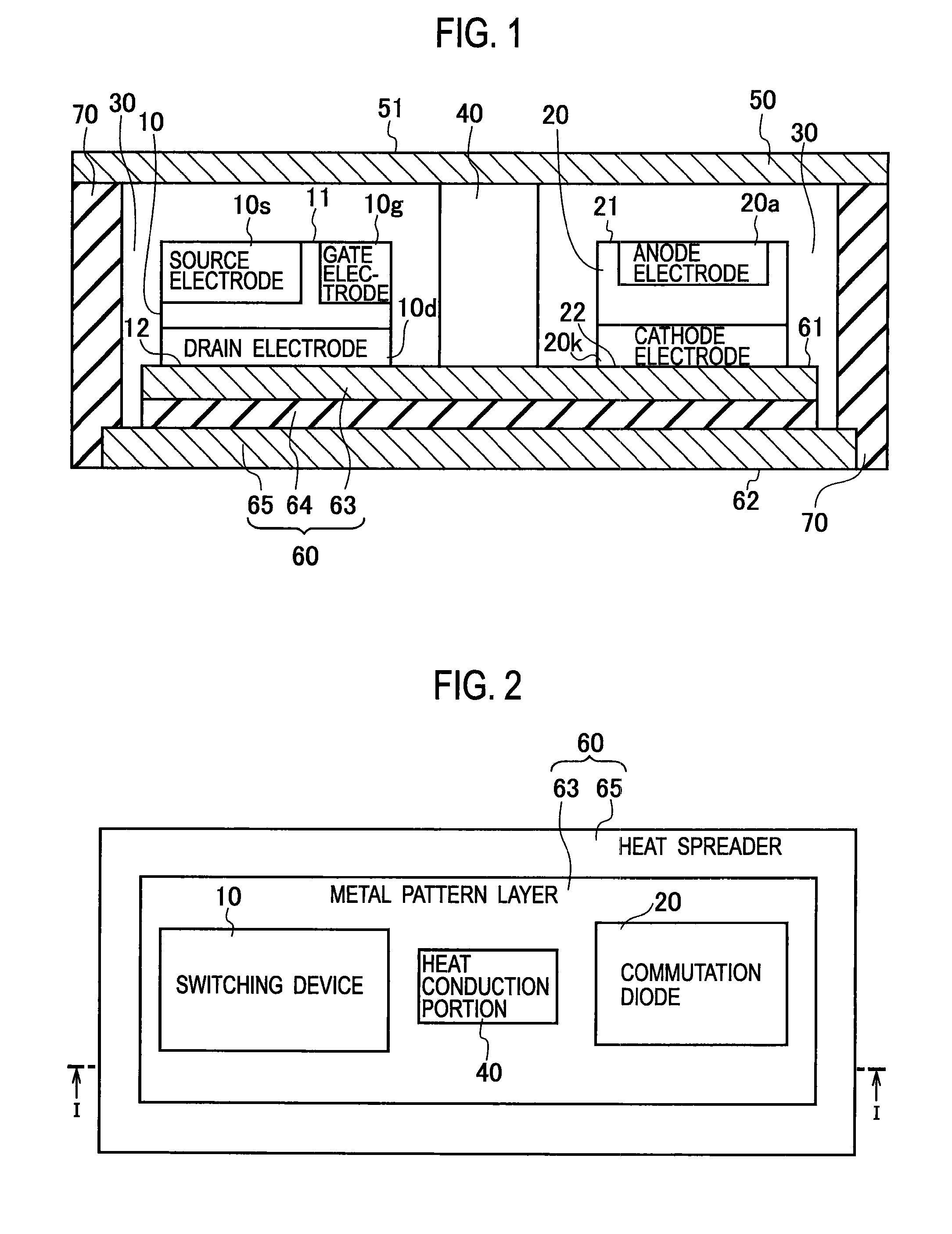
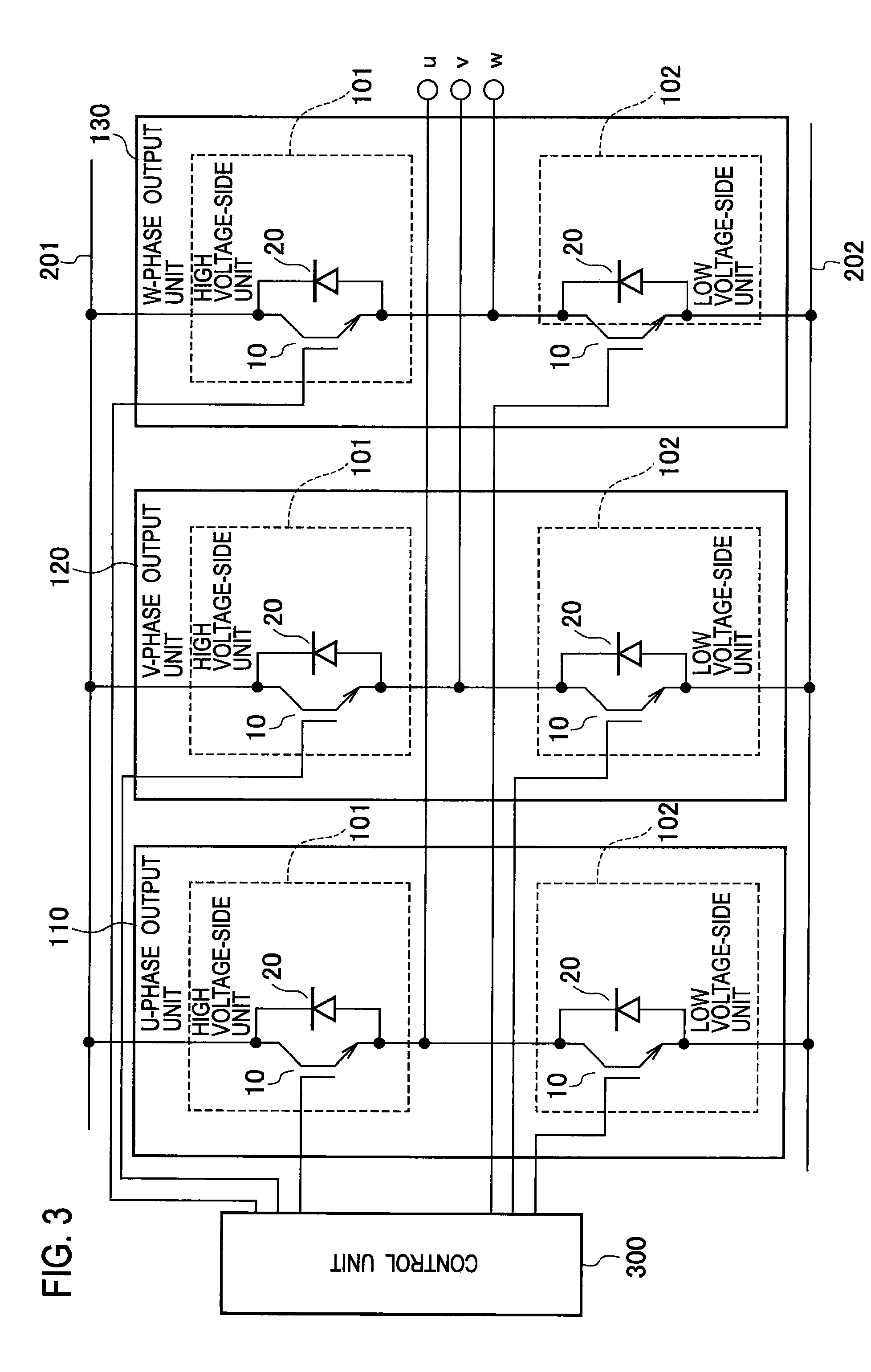
[0018]As shown in FIG. 1, a power module according to a first embodiment of the present invention includes: a substrate 60 having a first main substrate surface 61 and a second main substrate surface 62 opposite with the first main substrate surface 61; a switching device 10 and a commutation diode 20, which are arranged on the first main substrate surface 61; a heat conduction portion 40 disposed on the first main substrate surface 61 in a residual region of regions on which the switching deice 10 and the commutation diode 20 are arranged; and an upper cooling portion 50 disposed on the heat conduction portion 40.

[0019]The switching device 10 has a first main surface 11 on which a first main electrode (source electrode 10s) is formed, and a second main surface 12 on which a second main electrode (drain electrode 10d) in contact with the first main substrate surface 61 is formed, the second main surface 12 being opposite with the first main surface 11. The commutatio...

Example

SECOND EMBODIMENT

[0041]A power module according to a second embodiment of the present invention is different from the power module shown in FIG. 1 in that the heat conduction portion 40 is in contact with the heat spreader 65 of the substrate 60 as shown in FIG. 4. FIG. 5 shows a plan view of the power module shown in FIG. 4. FIG. 4 is a cross-sectional view taken along a II-II direction of FIG. 5. While seeing through the upper cooling portion 50, FIG. 5 shows the substrate 60, the switching device 10 and the commutation diode 20, and the heat conduction portion 40. In FIG. 5, the case 70 and the respective electrodes of the switching device 10 and the commutation diode 20 are not shown.

[0042]As shown in FIG. 4 and FIG. 5, an opening portion is provided in the metal pattern layer 63 and insulating layer 64 of the substrate 60, and the end portion of the heat conduction portion 40 is in contact with the surface of the heat spreader 65, which is exposed in the opening portion concern...

Example

THIRD EMBODIMENT

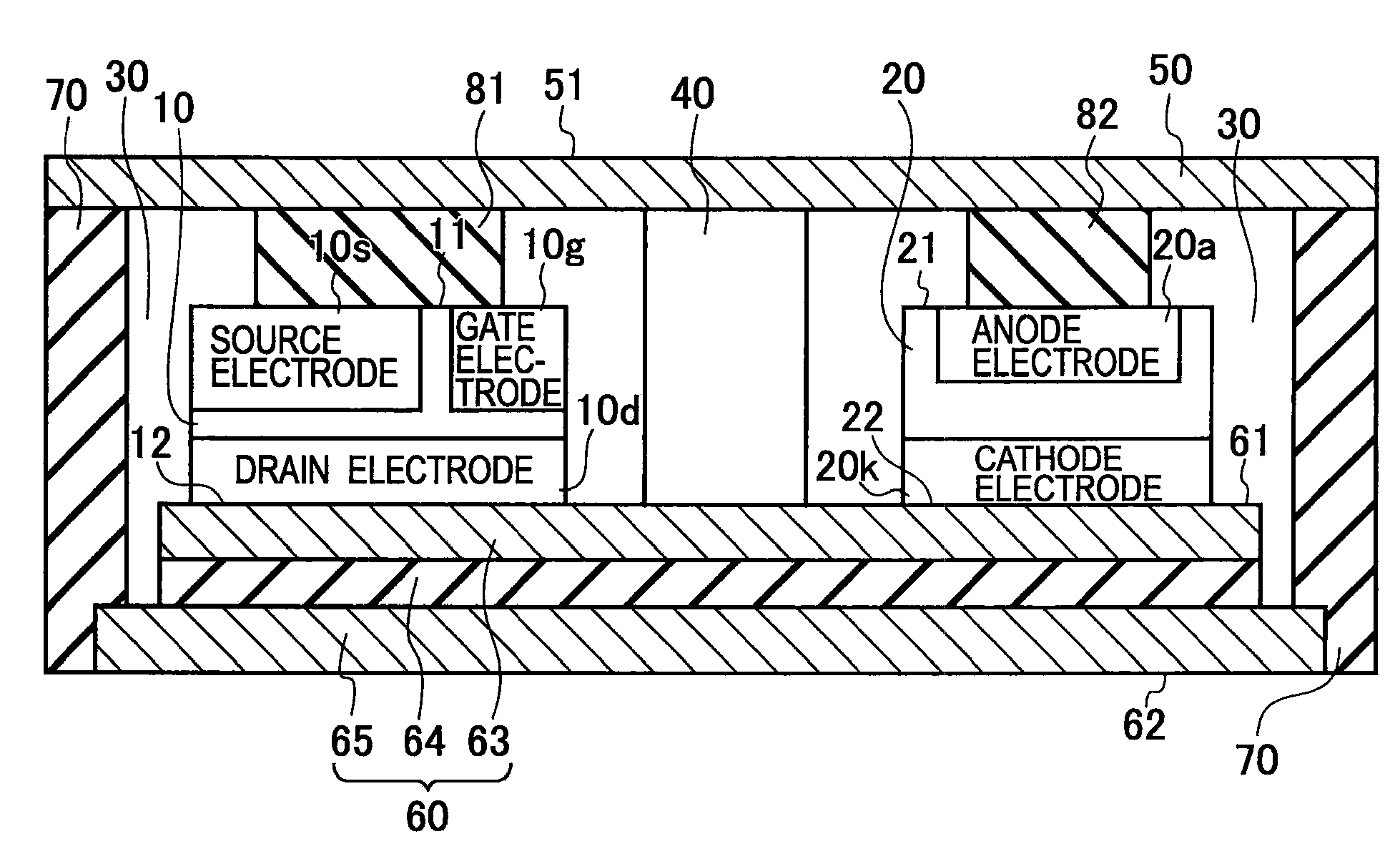
[0045]A power module according to a third embodiment of the present invention is different from the power module shown in FIG. 1 in that, as shown in FIG. 6, there are further provided: an upper joining portion 81, which is disposed on the first main surface 11 of the switching device 10 and is brought into contact with the upper cooling portion 50; and an upper joining portion 82, which is disposed on the first main surface 21 of the commutation diode 20, and is brought into contact with the upper cooling portion 50. Other configurations are substantially similar to those of the first embodiment shown in FIG. 1.

[0046]FIG. 7 shows a plan view of the power module shown in FIG. 6. While seeing through the upper cooling portion 50, FIG. 7 shows the substrate 60, the switching device 10, the commutation diode 20, the heat conduction portion 40, and the upper joining portions 81 and 82. As shown in FIG. 7, the upper joining portion 81 is disposed on the first main surface...


PUM


Abstract

A power module includes a substrate having first and second main substrate surfaces; a semiconductor device disposed on the first main substrate surface, and having a first main surface on which a first main electrode is formed, and a second main surface on which a second main electrode in contact with the first main substrate surface is formed; a heat conduction portion disposed on the first main substrate surface in a residual region of a region on which the semiconductor device is disposed; and an upper cooling portion disposed on the heat conduction portion.

Description

CROSS REFERENCE TO RELATED APPLICATIONS AND INCORPORATION BY REFERENCE[0001]This application is based upon and claims the benefit of priority from prior Japanese Patent Application P2007-258745 filed on Oct. 2, 2007 and prior Japanese Patent Application P2008-250388 filed on Sep. 29, 2008; the entire contents of which are incorporated by reference herein.BACKGROUND OF THE INVENTION[0002]1. Field of the Invention[0003]The present invention relates to a power module that converts a direct current into an alternating current, and particularly to a power module in which a semiconductor device is mounted on a substrate.[0004]2. Description of the Related Art[0005]A power module switches a switching device such as an insulating gate bipolar transistor (IGBT), thereby converts a direct current supplied from a direct current power supply into an alternating current, and drives an alternating-current motor or the like by the alternating current. In particular, a power module with which a con...

Claims


Application Information

Patent Timeline
IPC IPC(8): H01L23/34H01L29/739
CPCH01L23/3675H01L25/18H01L2924/0002H01L2924/00
Inventor SAITO, MASAOOTSUKA, TAKUKAZUOKUMURA, KEIJI
Owner ROHM CO LTD
Why Eureka
Try Eureka