Thin-film transistor

a transistor and thin film technology, applied in the field of thin film transistors, can solve the problems of difficult photolithography technique use, low carrier mobility, and difficult to carry, and achieve the effects of suppressing the diffusion of impurities, high mutual conductance, and high field-effect mobility

Inactive Publication Date: 2009-04-23
ZHANG HONGYONG +1
View PDF76 Cites 25 Cited by
  • Summary
  • Abstract
  • Description
  • Claims
  • Application Information

AI Technical Summary

Benefits of technology

[0017]In order to solve the above problems, in this invention an insulation layer 500 Å to 5000 Å thick is formed on the glass substrate as a bottom protective film before the TFT elements are formed, and the TFT elements are formed on top of this protective film. In this structure, it is possible to keep the impurities existing in the glass substrate from going into the active layer of a thin-film transistor or into the transistor elements themselves, and to provide a thin-film transistor that has high mutual conductance and high field-effect mobility. Also it suppresses the diffusion of impurities from the substrate which occurs when heat is generated during operation of the device. It also provides a thin-film transistor that can control degeneration of the electrical characteristics and has long-term stability and reliability.
[0018]Also by adding a halogen element to the protective film or to the gate insulator, impurities intruded from the outside or impurities in the film can be neutralized. Interface states between the insulation layer and the semiconductor layer can also be reduced by the halogen element. This increases stability and reliability of the TFT.

Problems solved by technology

The non-single-crystal semiconductor, when compared to the single-crystal semiconductor, has disadvantages that the carrier mobility is very low and thus the response speed of the transistor is very slow due to the many grain boundaries.
However, when forming elements on a large area substrate, it is apparently difficult to use the photolithography technique in order that the space between the source and drain (this is essentially the channel length) should 10 μm or less, due to the precise process, yield, and manufacturing cost problems.
Consequently, effective means for shortening the channel length of the TFT have not been found.
This lowers the mobility of the semiconductor layer and changes the threshold value, making the characteristics of the device worse and has an adverse effect on the long-term reliability of the device.
Also, through operation of the TFT, the TFT produces heat which causes the temperature of the glass substrate to rise thus causing-impurities to be diffused from the substrate, which also has an adverse effect on the TFT.
Also, ions that exist in a reaction space during the sputtering collide with the surface of the active layer of the thin-film transistor, which causes a damage to the active layer.

Method used


Image

  • Thin-film transistor
  • Thin-film transistor
  • Thin-film transistor

Examples


embodiment 1

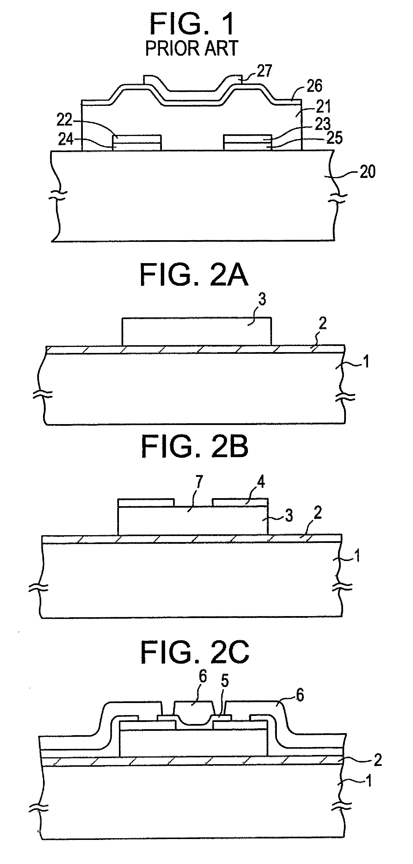
[0032]The manufacturing process of the planar type thin-film transistor in accordance with a first embodiment of the present invention is shown in FIG. 2(A) to FIG. 2(C).

[0033]First a glass substrate 1 is made of soda glass and on an entire surface of the substrate 1, a 300 nm thick silicon oxide bottom protective film 2 is formed by sputtering. The formation conditions of the film are shown below.

Sputtering Gasoxygen 100%Reaction Pressure 0.5 PaRF Power400 WSubstrate Temperature150° C.Film Formation Speed 5 nm / min

[0034]Next, an approximately 100 nm thick I-type conductivity non-single-crystal silicon semiconductor film 3 is formed by a CVD method on the protective film 2. The manufacturing conditions are shown below

Substrate Temperature 300° C.Reaction Pressure0.05 TorrRf Power (13.56 MHz)  80 WGas UsedSiH4

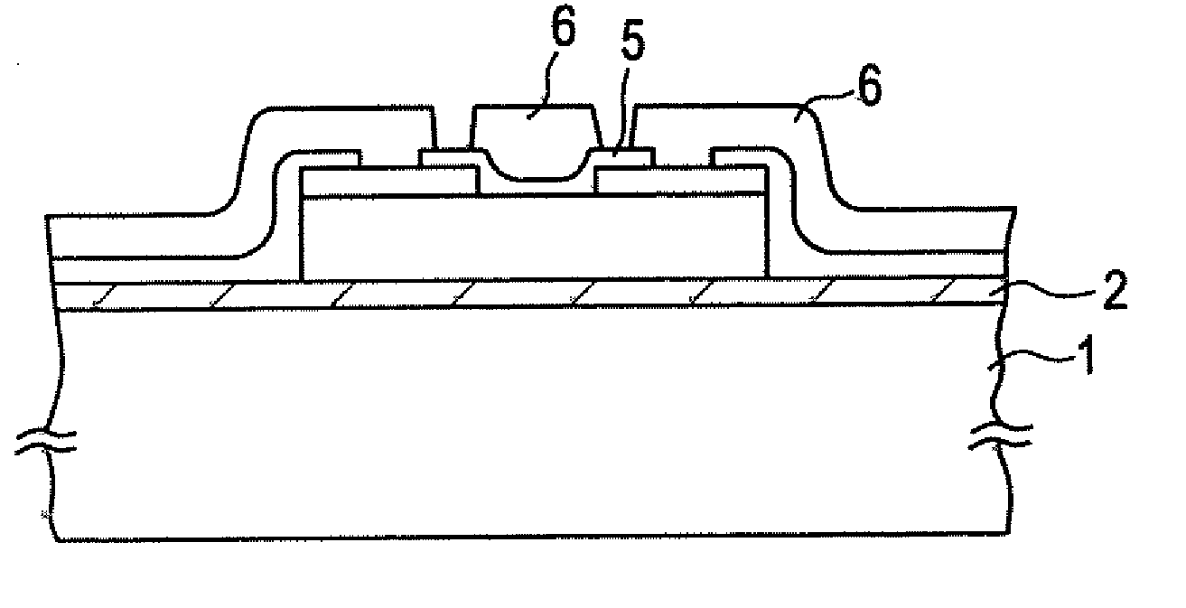
[0035]After this, a predetermined etching step is performed, so that the structure shown in FIG. 2(A) is obtained.

[0036]Next, in at least one region of the semiconductor film 3 t...

embodiment 2

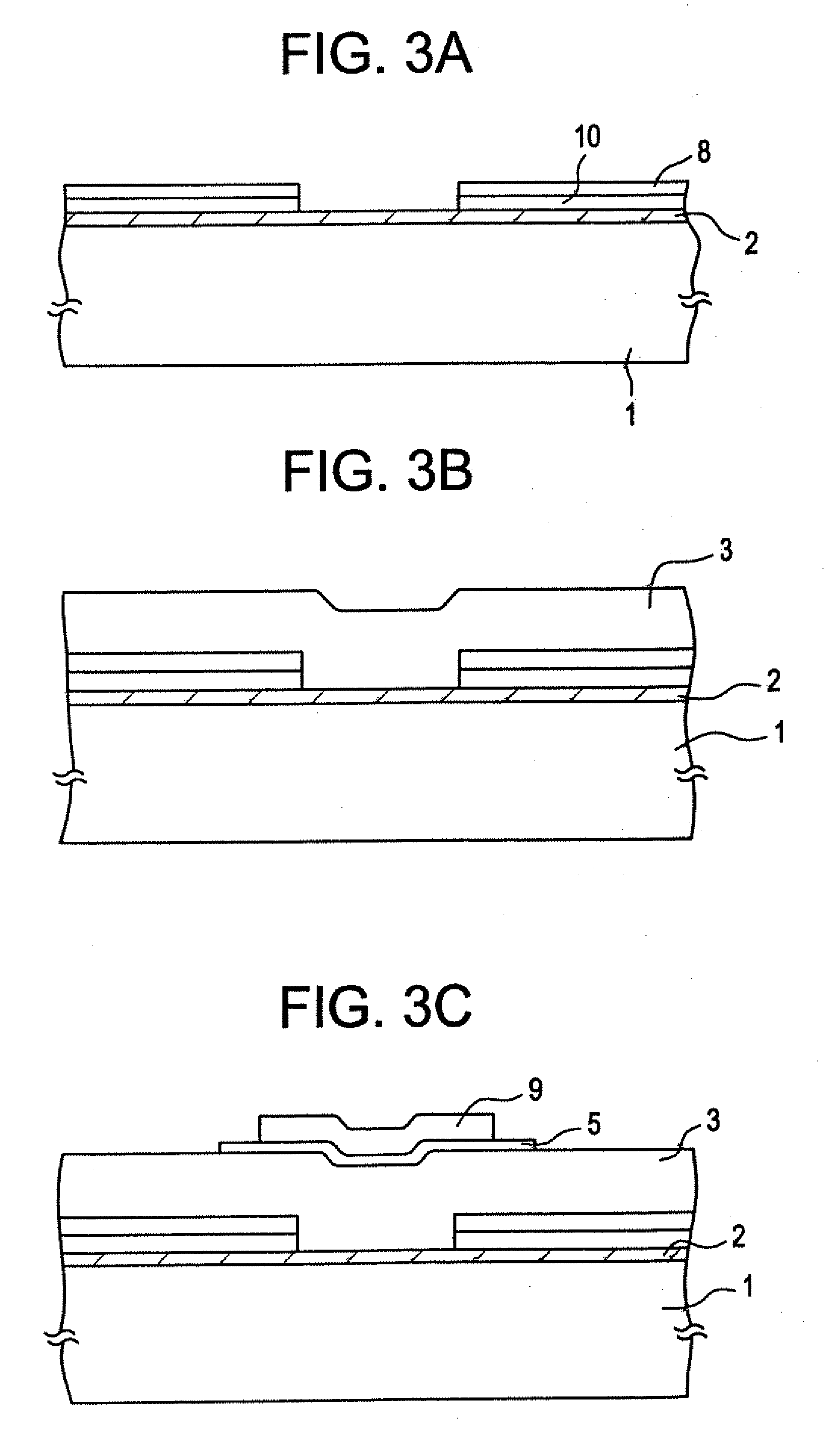
[0043]FIGS. 3A to 3C show a manufacturing process of an IG-FET in accordance with a second embodiment of the present invention. First, a 500 Å to 5000 Å thick silicon oxide film 2 is formed by a sputtering method on top of the soda glass substrate 1 as a protective film in a same manner as in Embodiment 1. Next, on the bottom protective film 2, a 200 nm thick molybdenum metallic layer 10 is formed. Formed on top of this structure is a non-single-crystal silicon film 8 which has a P-type conductor and has a low resistance. The formation conditions this time are as follows.

Substrate Temperature 230° C.Reaction Pressure0.05 TorrRf Power (13.56 MHz) 150 WGas UsedSi4 + B2H6Film Thickness 200 Å

[0044]This semiconductor layer can have ohmic contact with the I-type semiconductor layer that will be formed later in the process.

[0045]Next, a predetermined pattern is etched, and the structure shown in FIG. 3(A) is obtained. On top of this structure, a 200 nm thick I-type non-single-crystal silic...

embodiment 3

[0050]This embodiment will be explained referring to FIG. 4(A) to FIG. 4(D). In this embodiment a halogen element is added to the protective film on the glass substrate or to the gate insulator of the IG-FET or more preferably to the both.

[0051]In FIG. 4(A) a 200 nm thick SiO2 film 12 is formed on a glass substrate 11 using a magnetron-type RF sputtering method with the following formation conditions.

Reaction GasO2 95% volumeNF3 5% volumeFilm Formation Temperature150° C.RF Power (13.56 MHz)400 WPressure 0.5 PaSilicon is used as a target.

[0052]On top of this film 12, a 100 nm thick a-Si film 13 is formed by a magnetron RF sputtering in order to form a channel region, so that the structure shown in FIG. 4(A) is obtained. The film formation is done in an atmosphere of inert gas of argon and hydrogen and in the conditions shown below.

H2 / (H2 + Ar) =80% (partialpressure ratio)Film Formation Temperature150° C.RF Power (13.56 MHz)400 WTotal Pressure 0.5 Pa

Single crystal silicon is used as t...


PUM

PropertyMeasurementUnit
temperatureaaaaaaaaaa
lengthaaaaaaaaaa
temperatureaaaaaaaaaa

Abstract

A gate-insulated thin film transistor is disclosed. One improvement is that the thin film transistor is formed on a substrate through a blocking layer in between so that it is possible to prevent the transistor from being contaminated with impurities such as alkali ions which exist in the substrate. Also, a halogen is added to either or both of the blocking lay r and a gate insulator of the transistor.

Description

BACKGROUND OF THE INVENTION[0001]This invention relates to a thin-film transistor (from here on will also be referred to as a TFT) which is made of non-single-crystal semiconductor, for example an IG-FET, and its manufacturing process, and in more particular, to a highly reliable thin-film transistor which is suitable for use as a driving element of a display image sensor or liquid crystal device or the like.[0002]Thin-film transistors can be formed by a chemical vapor deposition method on an insulated substrate in a comparatively low temperature atmosphere, with a maximum temperature of 500° C., and the substrate being made of an inexpensive material such as soda glass or boron-silicate glass.[0003]This thin-film transistor is a field-effect transistor and has the same features as a MOSFET. In addition, as mentioned above, it has the advantage that it can be formed on an inexpensive insulated substrate at a low temperature. Also the thin film transistors can be formed on a large su...

Claims


Application Information

Patent Timeline
Patent Type & Authority Applications(United States)
IPC IPC(8): H01L29/72H01L21/336H01L21/77H01L21/84H01L29/49
CPCH01L27/1214H01L29/66757H01L29/4908Y10S148/118
Inventor ZHANG, HONGYONGYAMAZAKI, SHUNPEI
Owner ZHANG HONGYONG
Why Eureka
Try Eureka