Optical element and manufacturing method therefor

a manufacturing method and technology for optical elements, applied in the field of optical elements, can solve the problems of deterioration of optical elements with time, variation in luminance, and inability to achieve the effect of extending the life of the element, reducing the resistance of the cathode, and low resistivity

Inactive Publication Date: 2003-09-11
SANYO ELECTRIC CO LTD
View PDF21 Cites 1 Cited by
  • Summary
  • Abstract
  • Description
  • Claims
  • Application Information

AI Technical Summary

Benefits of technology

0048] The features of the present invention will be described below, based on the structure of the display pixel of the organic EL display apparatus described above. According to an embodiment of the present invention, the cathode 67 is made of aluminum. The resistance of the cathode can be lowered by forming the cathode with an aluminum which has a low resistivity.
0049] Moreover, a lithium fluoride layer is provided between the electron transport layer 65 and the cathode 67. This arrangement raises the injection efficiency of electrons injected from the cathode 67 into the electron transport layer 65, thereby extending the lifetime of the element.
0050] It is to be noted here that aluminum to form the cathode 67 is selected from ones with high purity. The purity of aluminum is preferably 99.9% or above. Moreover, the lithium fluoride layer and the cathode 67 are formed by vapor deposition under reduced pressure of 1.times.10.sup.-4 Pa or below. Through this process, impurities in the lithium fluoride layer and the cathode 67 are reduced. As a result, impurities do not segregate at these interfaces and thus the degradation of the element can be prevented. Moreover, the effects of impurities on the electron transport layer 65, the luminescent layer 63 and so forth can be eliminated, thus further contributing to the prevention of the element degradation. The pressure reduction at the vapor deposition of the lithium fluoride layer and the cathode 67 is carried out using a cryopump. Impurities such as carbon can be reduced by the use of the cryopump.
0051] In particular, the cathode 67 is formed by performing a vapor deposition of aluminum under reduced pressure within a normal temperature range between 20.degree. C. to 40.degree. C. both inclusive. Vapor deposition at normal temperatures like this allows the surface orientation of the aluminum to become (111), which is stable. Moreover, as described above, the vapor deposition under reduced pressure prevents a disarray of surface orientation due to the presence of impurities, so that the cathode 67 can be formed with an aluminum having a substantially uniform surface orientation. The vapor deposition at normal temperatures suppresses the diffusion of impurities adhering to the substrate, thus producing the effect of suppressing the diffusion of these impurities to the interface between the luminescent layer 66 and the cathode 67.
0052] After the formation of the cathode 67, the cathode 67 is subjected to a heating treatment at 50.degree. C. to 100.degree. C. both inclusive. This process further removes impurities such as water content, thus stabilizing the organic EL element 60.
0053] It should be noted here that, as have been described, the cathode 67 is formed for all the luminous element layers 66 of each display pixel, so that the current density drops so as to prevent electromigration.

Problems solved by technology

As a problem, the electron transport layer and luminescent layer in the organic EL elements structured as above are liable to be affected by impurities such as water molecules and oxygen molecules, and the deterioration thereof with time is generally conspicuous compared to LCDs or the like.
Moreover, it is difficult to stably inject electrons into the luminescent layer, so that there is a problem where variation in luminance is caused.
However, aluminum has a problem that the work function thereof may vary with the surface orientation thereof.
The unevenness of work function in the cathode causes the probability of injection of electrons from a position with lower work function, and thus a marked degradation is caused at the position.
Moreover, variation in work function in the cathode as a whole presents a problem of correspondingly varied electron injection efficiency, which causes uneven brightness by affecting the luminance of the optical element.

Method used


Image

  • Optical element and manufacturing method therefor
  • Optical element and manufacturing method therefor
  • Optical element and manufacturing method therefor

Examples


Embodiment Construction

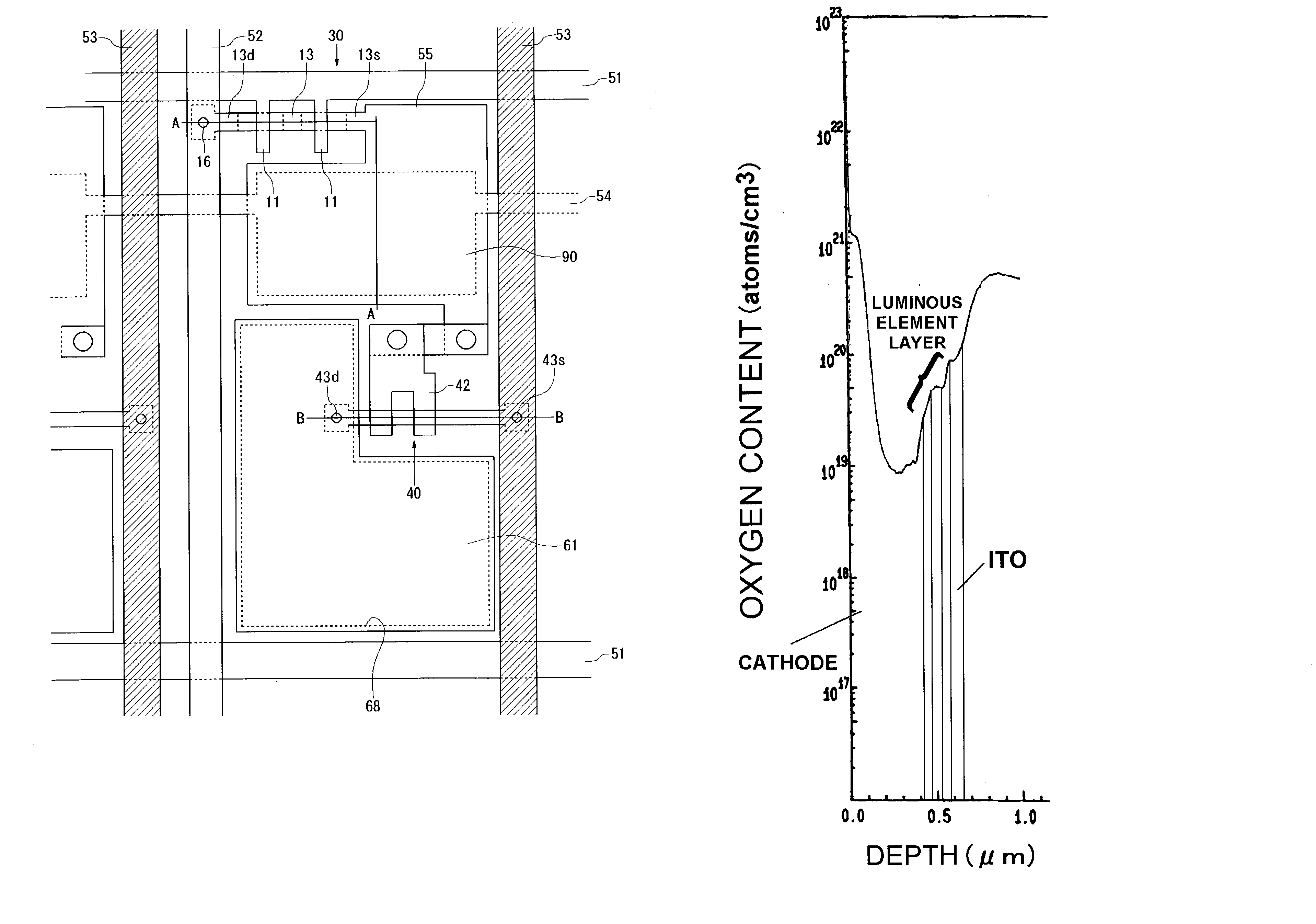
[0054] An example of method of forming of the cathode 67 will be described hereinbelow.

[0055] A substrate with an electron transport layer 65 formed thereon was introduced into a chamber, where the ambience was brought into a reduced pressure of 5.times.10.sup.-5 Pa by a load-lock type cryopump. In this low pressure ambience, lithium fluoride was vapor-deposited in a 1 nm-thick film on the electron transport layer 65. While maintaining this reduced pressure condition, aluminum was vapor-deposited into a 400 nm thickness on the lithium fluoride film at 30.degree. C. The aluminum used was of high purity (99.9% or above).

[0056] Thereafter, the substrate was heat-treated at 80.degree. C. for 60 minutes without being exposed to atmospheric air. This step is a preprocessing for the sealing, with metal or glass, of a cathode side of the entire organic EL display together with desiccant after the formation of the cathode.

[0057] The thickness of the lithium fluoride film can be achieved in t...


PUM

PropertyMeasurementUnit
thicknessaaaaaaaaaa
temperatureaaaaaaaaaa
work functionaaaaaaaaaa

Abstract

The cathode of an optical element, which is formed by a substrate, an anode formed on the substrate, a luminous element layer and a cathode, is made of aluminum whose surface orientation is substantially uniform. Oxygen content of the aluminum is substantially less or equal to 1x10²⁰ atoms/cm3.

Description

[0001] 1. Field of the Invention[0002] The present invention relates to optical elements and a method of manufacturing the optical elements.[0003] 2. Description of the Related Art[0004] Recently, organic electroluminescent (EL) display apparatus employing organic light emitting diodes (hereinafter referred to as OLED) as luminous elements are attracting much attention as display apparatus to replace CRTs and LCDs.[0005] Holes and electrons are injected to a luminescent layer from an anode formed on a glass substrate and a cathode provided above the anode, respectively. Then, these holes and electrons recombine with each other so as to produce excitons. And in the process of radiation deactivation of the excitons, light emanates from the luminescent layer and the organic EL element thus emits the light. It is to be noted here that a hole transport layer is provided between the anode and the luminescent layer whereas an electron transport layer is provided between the cathode and the...

Claims


Application Information

Patent Timeline
Patent Type & Authority Applications(United States)
IPC IPC(8): H01L27/32H01L51/50H05B33/26H01L51/52H05B33/10
CPCH01L27/3244H01L51/5221H01L51/5092H10K59/12H10K50/171H10K50/826H05B33/26
Inventor IDE, DAISUKESUZUKI, KOJI
Owner SANYO ELECTRIC CO LTD
Why Eureka
Try Eureka