Organic light emitting display and method of fabricating the same

a light-emitting display and organic technology, applied in the manufacture of electric discharge tubes/lamps, discharge tubes luminescnet screens, semiconductor/solid-state device details, etc., can solve the problems of serious luminance non-uniformity in the inside of the panel, high luminance emission of current injection, and difficulty in properly implementing the display. to achieve the effect of reducing the resistance of a cathode electrod

Active Publication Date: 2010-09-16
SAMSUNG DISPLAY CO LTD
View PDF9 Cites 15 Cited by
  • Summary
  • Abstract
  • Description
  • Claims
  • Application Information

AI Technical Summary

Benefits of technology

[0023]An organic light emitting display and a method of fabricating the same, in which the resistance of a cathode electrode is reduced by applying a conductive ink material on the cathode electrode, is provided in embodiments according to the present invention.

Problems solved by technology

Here, in the case of the top emission type organic light emitting display, the voltage drop is caused by the high resistance of the thin, transflective cathode electrode, making it difficult to properly implement the display.
In other words, a cathode electrode having a high resistance can result in a serious luminance non-uniformity in the inside of the panel and, particularly in large-area organic light emitting displays, a voltage drop (IR drop) occurs between the center portion and the outer portion of the panel, restricting current injection for high luminance emission in a high definition display.

Method used


Image

  • Organic light emitting display and method of fabricating the same
  • Organic light emitting display and method of fabricating the same
  • Organic light emitting display and method of fabricating the same

Examples


Embodiment Construction

[0032]In the following detailed description, only certain exemplary embodiments of the present invention are shown and described, simply by way of illustration. Here, when a first element is described as being coupled to a second element, the first element may be directly coupled to the second element, or may be indirectly coupled to the second element via a third element. Further, some of the elements that are not essential to obtain a complete understanding of the invention have been omitted for clarity. Like reference numerals refer to like elements throughout.

[0033]Hereinafter, exemplary embodiments of the present invention will be described in more detail with reference to the accompanying drawings.

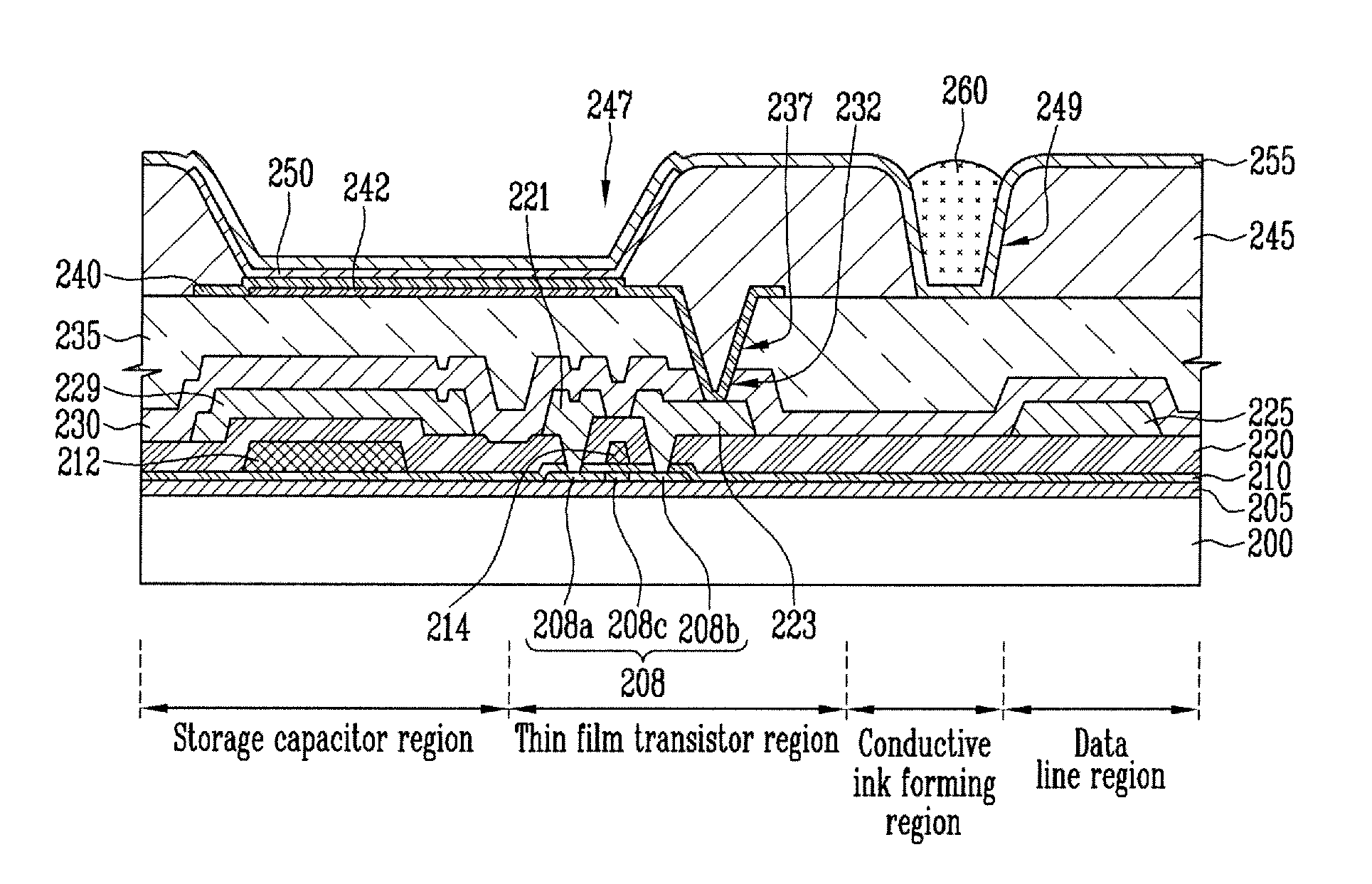
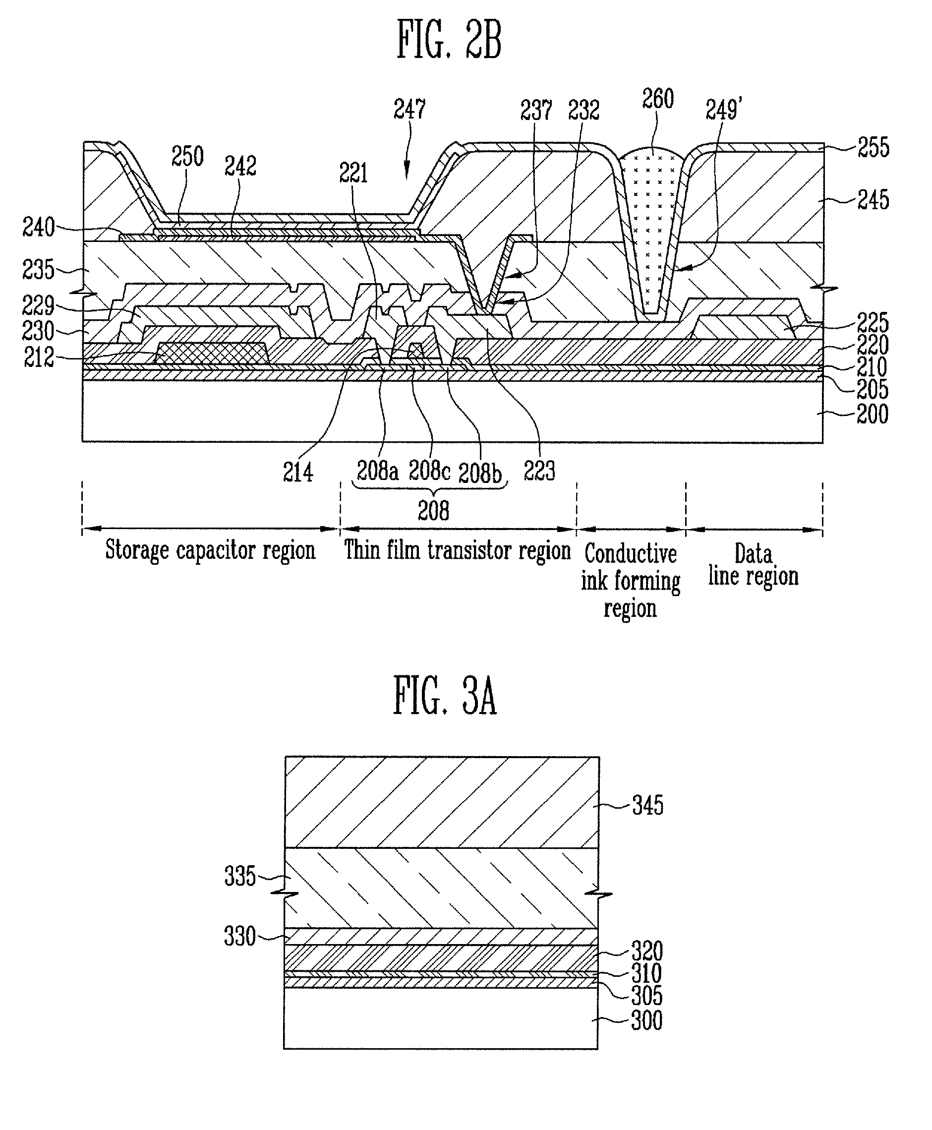
[0034]FIGS. 2A and 2B are cross-sectional views of an organic light emitting display according to exemplary embodiments of the present invention.

[0035]FIG. 2A illustrates a pixel region including a storage capacitor region and a thin film transistor region, a conductive ink forming r...


PUM


Abstract

An organic light emitting display and a method of fabricating the same, in which the resistance of a cathode electrode is reduced by applying a conductive ink material on the cathode electrode. A pixel defining layer is formed on a substrate, with a recess or depression in a non-light emitting region of the pixel defining layer. An electrode on the substrate includes a portion within the recess of the pixel defining layer. The conductive ink is in the portion of the electrode in the recess.

Description

CROSS-REFERENCE TO RELATED APPLICATIONS[0001]This application claims priority to and the benefit of U.S. Provisional Patent Application No. 61 / 079,023, filed on Jul. 8, 2008, the entire content of which is incorporated herein by reference.BACKGROUND[0002]1. Field of the Invention[0003]The present invention relates to an organic light emitting display, and a method of fabricating the same.[0004]2. Discussion of Related Art[0005]Generally, electroluminescence displays, which are self-luminous displays, electrically excite fluorescent materials to emit light. These electroluminescence displays have generated significant interest as next-generation displays due to advantages such as low voltage operation, a very slim form factor, a wide viewing angle, a high speed response, etc., which are advantages that generally cannot be achieved in liquid crystal displays.[0006]Electroluminescence displays include inorganic light emitting displays and organic light emitting displays, depending on w...

Claims


Application Information

Patent Timeline
Patent Type & Authority Applications(United States)
IPC IPC(8): H01J1/63H01J9/02
CPCH01L51/0022H01L27/3276H10K71/135H10K71/611H10K59/131H01L21/02288H01L21/7684H01L23/4828H10K59/122
Inventor SONG, MYUNG-WON
Owner SAMSUNG DISPLAY CO LTD
Why Eureka
Try Eureka