Organic light emitting display device and method of manufacturing the same

a technology of organic light and display device, which is applied in the direction of semiconductor devices, basic electric elements, electrical appliances, etc., can solve the problems of increasing complicated manufacturing process, and achieve the effect of reducing the resistance of the cathode electrode, simplifying the manufacturing process, and reducing the number of masks

Active Publication Date: 2017-05-04
LG DISPLAY CO LTD
View PDF3 Cites 17 Cited by
  • Summary
  • Abstract
  • Description
  • Claims
  • Application Information

AI Technical Summary

Benefits of technology

[0014]An aspect of the present invention is directed to provide a top emission type transparent organic light emitting display device and a method of manufacturing the same, which provides an area of an auxiliary electrode that effectively reduces a resistance of a cathode electrode, and decreases the number of masks, thereby simplifying the manufacturing process.

Problems solved by technology

However, when the TFT layer T is stacked in the emissive part, an auxiliary electrode cannot be stacked in the emissive part, and for this reason, the auxiliary electrode should be stacked separately from the TFT layer T. Two auxiliary electrodes should be vertically stacked for stacking the two auxiliary electrodes in a limited space.
Also, since separate masks are used for stacking the two auxiliary electrodes on one layer, the number of masks increases, and for this reason, a manufacturing process becomes complicated.

Method used


Image

  • Organic light emitting display device and method of manufacturing the same
  • Organic light emitting display device and method of manufacturing the same
  • Organic light emitting display device and method of manufacturing the same

Examples


Embodiment Construction

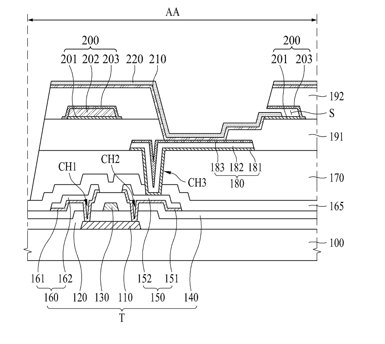
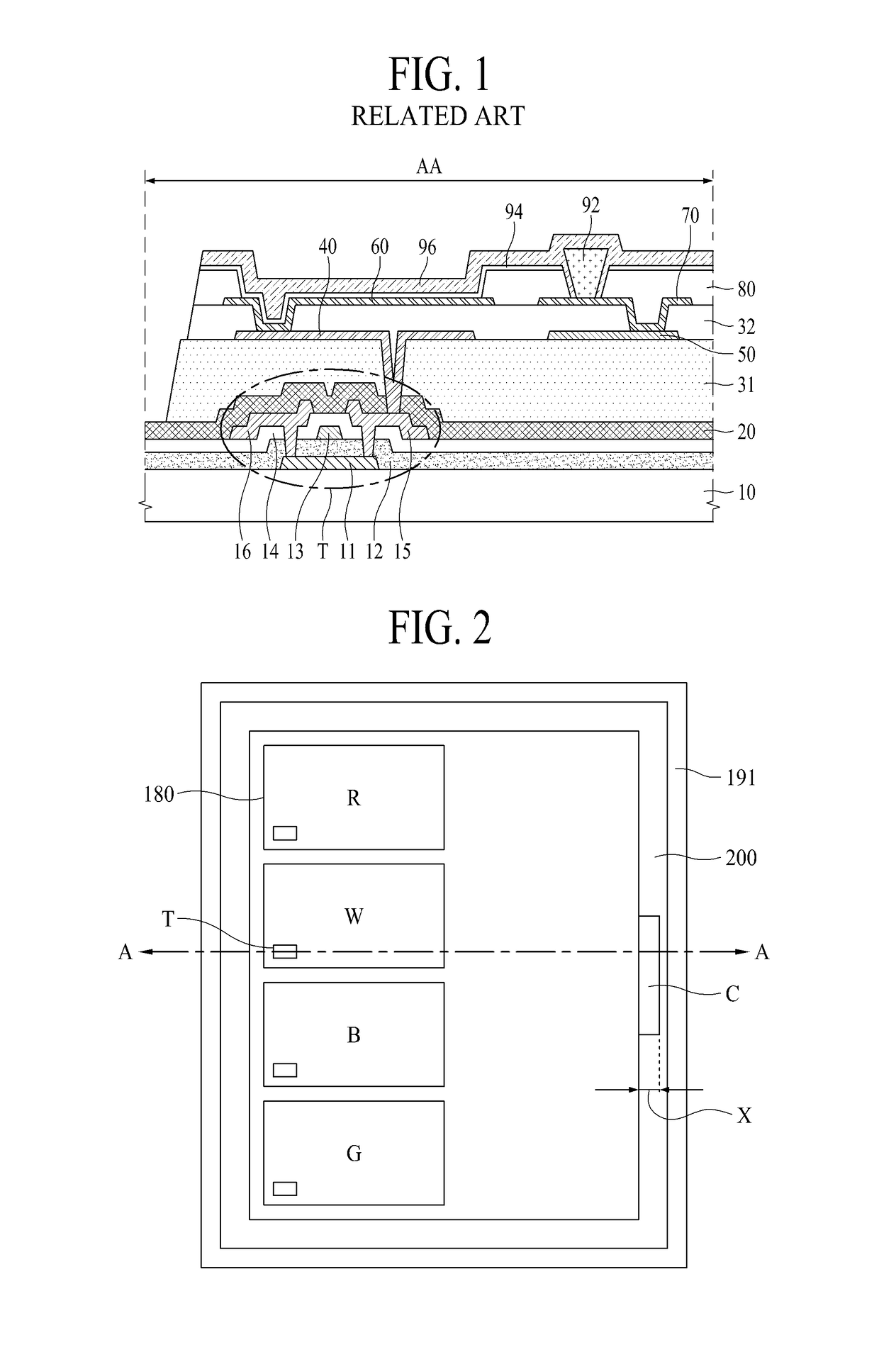
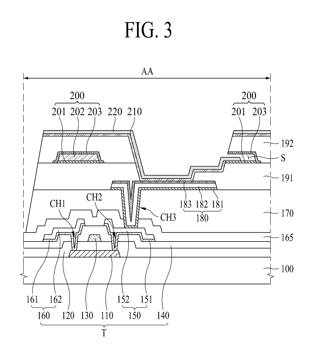
[0024]Reference will now be made in detail to the exemplary embodiments of the present invention, examples of which are illustrated in the accompanying drawings. Wherever possible, the same reference numbers will be used throughout the drawings to refer to the same or like parts.

[0025]Advantages and features of the present invention, and implementation methods thereof will be clarified through following embodiments described with reference to the accompanying drawings. The present invention may, however, be embodied in different forms and should not be construed as limited to the embodiments set forth herein. Rather, these embodiments are provided so that this disclosure will be thorough and complete, and will fully convey the scope of the present invention to those skilled in the art. Further, the present invention is only defined by scopes of claims.

[0026]A shape, a size, a ratio, an angle, and a number disclosed in the drawings for describing embodiments of the present invention ...


PUM


Abstract

Discussed is an organic light emitting display device according to the embodiments. The organic light emitting display device includes an anode electrode in each of a plurality of pixels defined on a substrate, a bank and an organic emission layer on the anode electrode, a cathode electrode on the organic emission layer, and an auxiliary electrode connected to the cathode electrode. The auxiliary electrode is provided on the bank, thereby the auxiliary electrode is disposed on a layer different from the anode electrode.

Description

CROSS-REFERENCE TO THE RELATED APPLICATIONS[0001]This application claims the priority benefit of the Korean Patent Application No. 10-2015-0151375 filed on Oct. 29, 2015, which is hereby incorporated by reference as if fully set forth herein.BACKGROUND OF THE INVENTION[0002]Field of the Invention[0003]The present invention relates to an organic light emitting display device, and more particularly, to a top emission type transparent organic light emitting display device and a method of manufacturing the same.[0004]Discussion of the Related Art[0005]Organic light emitting display devices are self-emitting devices and have low power consumption, a fast response time, high emission efficiency, high luminance, and a wide viewing angle. The organic light emitting display devices are classified into a top emission type and a bottom emission type, based on a transmission direction of light emitted from an organic light emitting device. In the bottom emission type, a circuit element is dispo...

Claims


Application Information

Patent Timeline
Patent Type & Authority Applications(United States)
IPC IPC(8): H01L27/32H01L51/56H01L51/52
CPCH01L27/3276H01L27/3248H01L27/3246H01L27/3213H01L51/56H01L51/5228H01L51/5218H01L51/5221H10K59/00H10K59/131H10K59/1201H10K59/1315H10K59/122H10K50/814H10K50/818H10K50/824H10K50/82H10K59/123H10K59/351H10K71/00
Inventor LEE, JOONSUKKIM, SEJUNE
Owner LG DISPLAY CO LTD
Why Eureka
Try Eureka