Solid-state imaging device

a solid-state imaging and circuit technology, applied in the field of signal processing circuits, can solve the problems of not being able to mount frame memory, not being able to perform enlargement zoom, and mos-type sensor facing the above-described problems, so as to achieve the effect of simplifying the interface between the digital picture signal and the circuit or the device to be connected thereto

Active Publication Date: 2009-09-10
GK BRIDGE 1
View PDF10 Cites 13 Cited by
  • Summary
  • Abstract
  • Description
  • Claims
  • Application Information

AI Technical Summary

Benefits of technology

[0011]With this configuration, it is possible to achieve the electronic enlargement zoom even without a frame memory under a condition where the output size to the picked-up size is one or more times.
[0013]According to this construction, it is possible to achieve the electronic enlargement zoom even without a frame memory and, moreover, without performing high-rate transfer and intermittent readout by the solid-state imaging device under a condition where the output size to the picked-up size is one or more times.
[0015]According to this, the synchronizing signal of the digital picture signal outputted from the processing unit for picture signal can be provided with a uniform periodicity regardless of the zoom magnifications and without intermittence. Therefore, the interface between the digital picture signal and the circuit or the device to be connected thereto can be simplified.

Problems solved by technology

However, it is not possible with this configuration to perform enlargement zoom when the size of the picked-up area 91 and that of the picked-up picture output area 92 are equal as shown in FIG. 10A.
Thus, it is not practical to mount the frame memory.
However, like the CCD, the MOS-type sensor faces the above-described problems.

Method used


Image

  • Solid-state imaging device
  • Solid-state imaging device
  • Solid-state imaging device

Examples


first embodiment

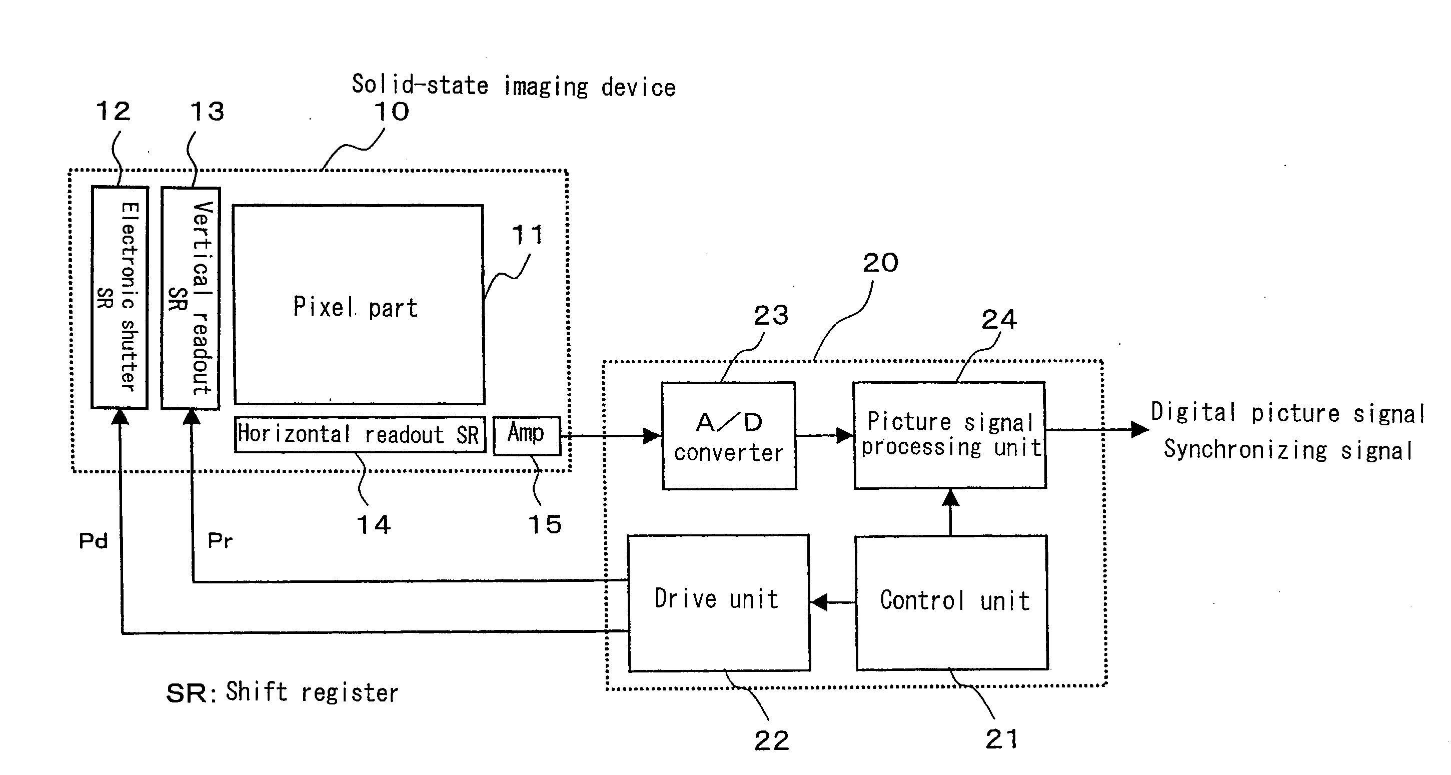
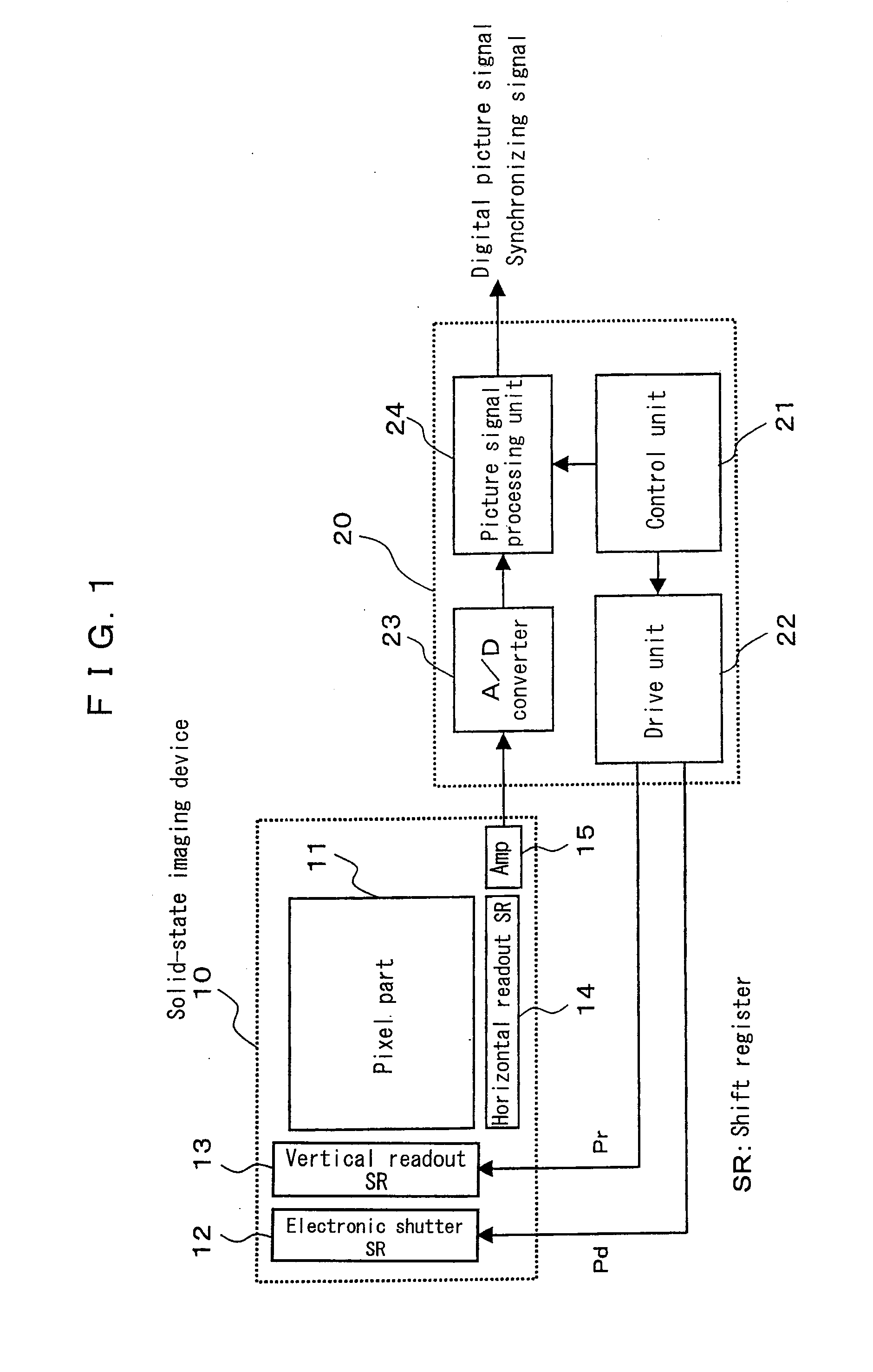
[0035]FIG. 1 is a block diagram for showing the structure of a solid-state imaging device according to a first embodiment of the present invention. The solid-state imaging device comprises a solid-state imaging device 10 and a signal processing circuit 20. The signal processing circuit 20 comprises a control unit 21, a drive unit 22, an A / D converter 23, and a processing unit for picture signal 24. The solid-state imaging device 10 comprises: a pixel part 11 arranged two-dimensionally; an electronic shutter shift register 12 for transferring electronic shutter shift pulse Pd in order; a vertical readout shift register 13 to transfer vertical readout shift pulse Pr for reading out an electric charge to the pixel part 11 in order; a horizontal readout shift register 14 to transfer the electric charge read out from the pixel part 11 in order to the horizontal direction; and an output amplifier 15.

[0036]The pixel part 11 is consisted of a random-accessible MOS-type sensor with a focal-p...

second embodiment

[0060]A second embodiment of the present invention achieves electronic enlargement zoom without performing the high-rate transfer and intermittent readout in the solid-state imaging device 10. The embodiment therefore is characterized by that the blanking period of the horizontal synchronizing signal (referred to as a horizontal blanking period hereinafter) is extended to be more than the valid period of the picture signal by the drive unit 22. The fundamental structure of the solid-state imaging device according to this embodiment is the same as that of the first embodiment shown in FIG. 1.

[0061]In the embodiment, as shown in the picture configuration of FIG. 7A, horizontal blanking period τ2 corresponding to “H” level of the horizontal synchronizing signal HD is extended to be more than picture signal valid period τ1. As a result, there appears an invalid signal area A2 in the periphery of the picture signal area A1. The horizontal line continues to the horizontal line of the next...

third embodiment

[0071]A third embodiment of the present invention allows the synchronizing signal to have the constant cycle regardless of the magnifications (zoom magnifications) in the electronic enlargement zoom. The fundamental structure of the solid-state imaging device according to this embodiment is the same as that of the first embodiment shown in FIG. 1.

[0072]When the electronic enlargement zoom is achieved by the constitutions of the first and second embodiments without using a frame memory, the occurrence cycle of the line intermittence (referred to as a line intermittence cycle hereinafter) varies in accordance with the zoom magnification. In FIG. 8, reference numeral HD3 is a horizontal synchronizing signal of the picture signal inputted from the solid-state imaging device 10. A horizontal synchronizing signal H4 at the magnification of ¾ times has a periodicity of one valid line, one invalid line, and two valid lines as a unit, however, it becomes in “H”, “L”, “H”, and “H”, which has ...


PUM


Abstract

The signal processing circuit of the present invention comprises a drive unit and a processing unit for picture signal. The drive unit supplies each of the shift pulses separately to the electronic shutter shift register and the readout shift register. The processing unit for picture signal designates a control start position of a digital picture signal outputted from an A / D converter and performs interpolation processing thereon along the horizontal direction and the vertical direction. The drive unit adjusts cycles of each of the shift pulses for controlling a vertical-line readout rate of the solid-state imaging device, and then intermittently reads out the analog picture signal from the solid-state imaging device. The processing unit for picture signal performs vertical-line interpolation processing in accordance with the vertical-line readout rate for extending a part of picture area of the digital picture signal.

Description

BACKGROUND OF THE INVENTION[0001]1. Field of the Invention[0002]The present invention relates to a signal processing circuit for a solid-state imaging device of a portable telephone with a built-in camera, a digital still camera, etc., and to a solid-state imaging device.[0003]2. Description of the Related Art[0004]Imaging devices such as a portable telephone, digital still camera and the like have an enlargement zoom mechanism mounted thereon as an essential function of the camera. As the enlargement zoom functions, there are an optical enlargement zoom function that zooms in and out by controlling a lens, and an electronic enlargement zoom mechanism that zooms by interpolation of digital data. The optical enlargement zoom mechanism tends to be large-scaled since it requires mechanisms such as a zoom lens and a motor to drive the zoom lens. Therefore, an electronic enlargement zoom mechanism of a smaller-scale is frequently used for a small-size imaging device such as a portable ca...

Claims


Application Information

Patent Timeline
Patent Type & Authority Applications(United States)
IPC IPC(8): H04N5/262H04N5/335H04N5/353H04N5/374H04N5/376H04N101/00
CPCG06T3/4007H04N3/155H04N1/3935H04N25/443H04N25/745
Inventor TAKAHASHI, KENJISASAKI, YOSHIMITSUNAKASHIMA, TOSHIYUKI
Owner GK BRIDGE 1
Why Eureka
Try Eureka