

Display substrate and method for manufacturing the same
- Summary
- Abstract
- Description
- Claims
- Application Information
AI Technical Summary
Benefits of technology
Problems solved by technology
Method used
Image

Examples
Example
Exemplary Embodiment 1
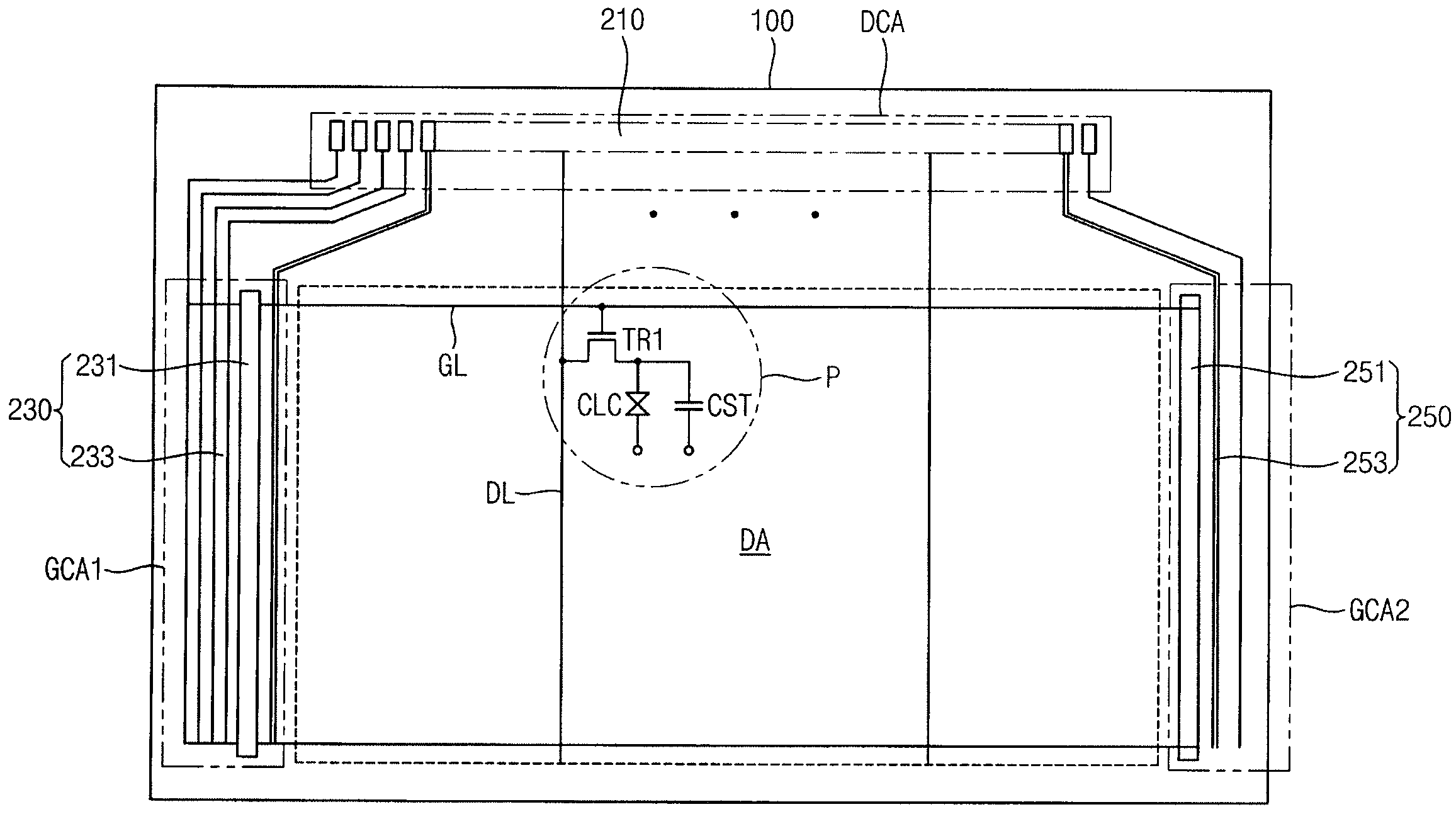
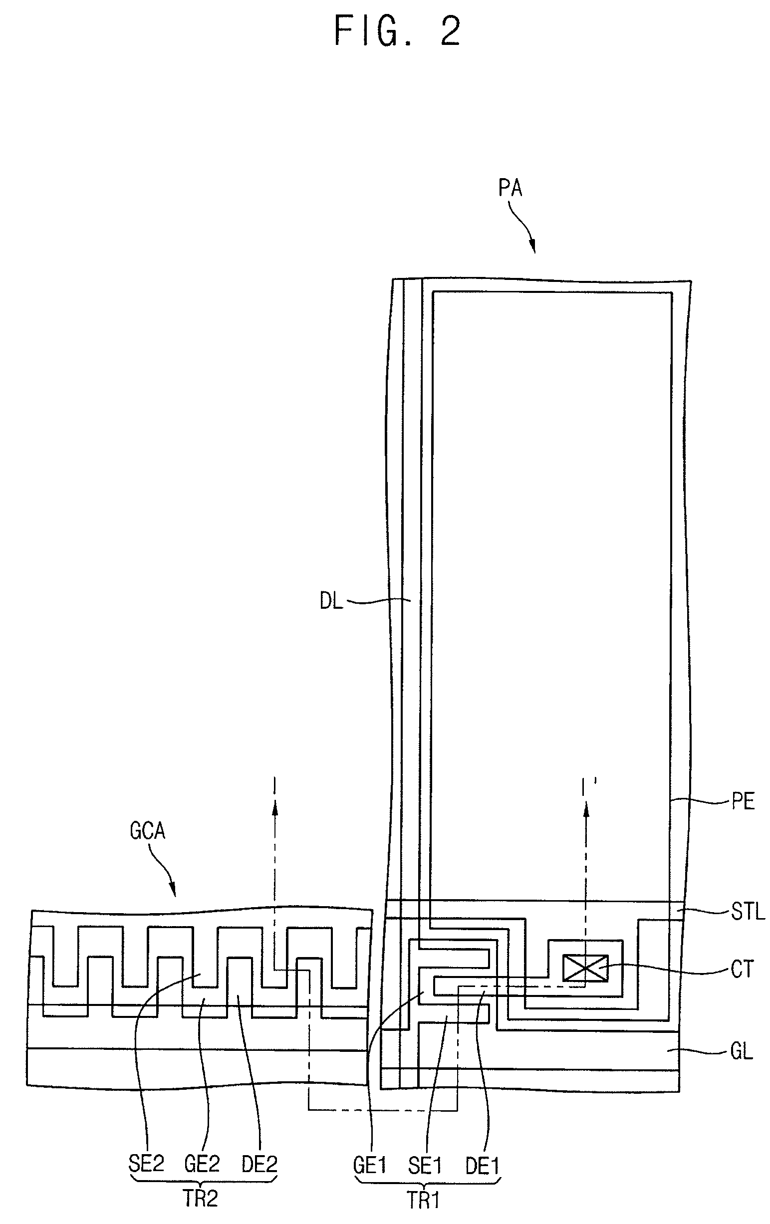
[0033]FIG. 1 is a plan view illustrating a display substrate according to Exemplary Embodiment 1 of the present invention. FIG. 2 is an enlarged view partially illustrating the display substrate in FIG. 1.
[0034]Referring to FIGS. 1 and 2, the display apparatus 100 includes a display area DA and a peripheral area surrounding the display area DA. The peripheral area has a data circuit area DCA and gate circuit areas GCA1 and GCA2. A plurality of pixel portions P is formed in the display area DA. Each of the pixel portions P includes a gate line GL, a data line DL crossing the gate line GL, a first switching element TRI electrically connected to the gate and data lines GL and DL, a liquid crystal capacitor CLC electrically connected to the first switching element TR1, and a storage capacitor CST.
[0035]The data circuit area DCA is defined as an area adjacent to a portion of the data line DL, and a data pad part 210 is formed in the data circuit area DCA. The data ...
Example
Exemplary Embodiment 2
[0065]FIG. 8 is a cross-sectional view illustrating a display substrate according to Exemplary Embodiment 2 of the present invention. The display substrate according to the present exemplary embodiment is substantially the same as the display substrate in Exemplary Embodiment 1 except for a circuit barrier pattern formed in the gate circuit area. Thus, the same reference numerals will be used to refer to the same or like parts as those described in Exemplary Embodiment 1 and any further repetitive explanation concerning the above elements will be omitted.
[0066]Referring to FIG. 8, the SLG substrate 101 includes the pixel area PA in which the pixel portion P is formed, and the gate circuit area GCA in which the gate circuit part is formed.
[0067]The barrier patterns are formed on the SLG substrate 101. The barrier patterns 111 and 113 patterned in substantially the same way as the first conductive pattern are formed in the pixel area PA to decrease the area of t...
PUM
| Property | Measurement | Unit |
|---|---|---|
| Electrical conductor | aaaaa | aaaaa |
| Area | aaaaa | aaaaa |
| Transparency | aaaaa | aaaaa |
Abstract
Description
Claims
Application Information