Side view light emitting diode package

a technology of light-emitting diodes and side views, which is applied in the direction of optics, optical elements, instruments, etc., can solve the problems of reducing the entire light quantity emitted out and degrading performance, so as to improve the beam angle characteristics of emission light, prevent a sidewall molding defect, and increase the light quantity

Inactive Publication Date: 2009-11-19
SAMSUNG ELECTRONICS CO LTD
View PDF7 Cites 5 Cited by
  • Summary
  • Abstract
  • Description
  • Claims
  • Application Information

AI Technical Summary

Benefits of technology

[0014]The present invention has been made to solve the foregoing problems of the prior art and therefore an aspect of the present invention is to provide a side view LED package in which the height of a sidewall is shortened to improve beam angle characteristics of emission light, increase light quantity, and prevent a molding defect of the sidewall.
[0018]In this case, the height of the wire from the top of the LED chip to the top of the wire can be reduced preferably to 100 μm or less, and more preferably to the order of 70 μm. Thus, the afore-described bonding is advantageous to set the cavity depth in a small value.

Problems solved by technology

First, this restricts the beam angle α of the light emitted out of the LED package 10. When the beam angle α is smaller, the backlight unit 1 should use the more LED packages 10.
Second, as can be seen from FIG. 5, when light beams L generated from the LED chip 12 are emitted in the direction of arrow A, a partial light beam L1 collides against a sidewall 17 of the LED package 10. When collided against the side wall 17, the light beam 17 is lost due to for example absorption / scattering. This reduces the entire light quantity emitted out of the LED package 10. The light quantity decreases more when the sidewall 17 is higher, that is, the cavity depth d in FIG. 4 is larger.
Third, the higher sidewall 17 may cause more easily a molding defect such as a void in an upper or lower portion of the sidewall 17. This may take place particularly in a portion designated with the reference sign I in FIG. 3. With the molding defect, the LED package 10 is degraded in performance, and sometimes, should be discarded.

Method used


Image

  • Side view light emitting diode package
  • Side view light emitting diode package
  • Side view light emitting diode package

Examples


Embodiment Construction

[0035]The present invention will now be described more fully hereinafter with reference to the accompanying drawings, in which preferred embodiments of the invention are shown.

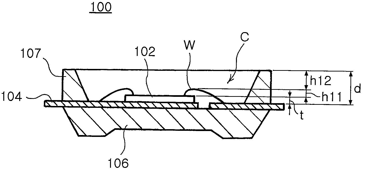
[0036]FIG. 6 is a cross-sectional view illustrating an LED package 100 according to an embodiment of the invention.

[0037]Referring to FIG. 6, the side view LED package 100 of the invention is applied to the backlight unit 1 as shown in FIG. 1. The LED package 100 includes an LED chip 102, first and second lead frames 104 for supplying power to the LED chip 102 seated thereon, a package body 106 injection-molded to hold the first and second lead frames 104 and an encapsulant 108 of a transparent resin filled in a cavity C of the package body 106 to encapsulate the LED chip 102.

[0038]The LED package 100 according to this embodiment of the invention has an improvement in the cavity C in order to improve light quantity and beam angle. The height of a sidewall of the LED package 100, that is, the depth d of the cav...


PUM


Abstract

A side view LED package for a backlight unit includes a package body having a cavity with an inclined inner sidewall, first and second lead frames arranged in the package body, the cavity of the package body exposing a portion of at least one of the first and second lead frames placed in a bottom of the cavity to outside, a light emitting diode chip mounted on the bottom of the cavity to be electrically connected to the first and second lead frames, and a transparent encapsulant arranged in the cavity surrounding the light emitting diode chip. The cavity has a depth larger than a mounting height of the light emitting diode chip and not exceeding six times of the mounting height. The height of the sidewall is shortened to improve beam angle characteristics of emission light, increase light quantity, and prevent a molding defect of the sidewall.

Description

CLAIM OF PRIORITY[0001]This application claims the benefit of Korean Patent Application No. 2005-113834 filed on Nov. 25, 2005, in the Korean Intellectual Property Office, the disclosure of which is incorporated herein by reference.BACKGROUND OF THE INVENTION[0002]1. Field of the Invention[0003]The present invention relates to a high power Light Emitting Diode (LED) package, particularly, in which the height of a sidewall is shortened to improve beam angle characteristics of emission light, increase light quantity, and prevent a molding defect of the sidewall.[0004]2. Description of the Related Art[0005]A Liquid Crystal Display (LCD) does not have a light source of its own, and thus requires an external illumination, which is generally referred to as a backlight unit. The backlight unit illuminates the LCD from the back and uses a Cold Cathode Fluorescent Lamp (CCFL) or an LED as a light source.[0006]FIGS. 1 and 2 show a general backlight unit 1 in use for the LCD. Referring to FIGS...

Claims


Application Information

Patent Timeline
Patent Type & Authority Applications(United States)
IPC IPC(8): H01L33/00H01L33/60H01L33/62
CPCG02B6/0073H01L33/483H01L33/60H01L33/62H01L2224/48091H01L2224/48465H01L2224/48471H01L2224/48247H01L2224/32245H01L2224/73265H01L2924/00014H01L2924/00H01L2224/48227H01L2224/4554H01L33/54
Inventor KIM, CHANG WOOKHAN, YOON SUKSONG, YOUNG JAEKIM, BYUNG MANROH, JAE KYHONG, SEONG JAE
Owner SAMSUNG ELECTRONICS CO LTD
Why Eureka
Try Eureka