Supercharge Your Innovation With Domain-Expert AI Agents!

Integrated circuit chip identification element

a technology of integrated circuit chips and identification elements, applied in the direction of measuring devices, instruments, electrical equipment, etc., can solve the problems of parameters that are likely to vary over time, and features that are sensitive to parasitic dispersions

Active Publication Date: 2010-12-23
STMICROELECTRONICS (ROUSSET) SAS
View PDF6 Cites 4 Cited by
  • Summary
  • Abstract
  • Description
  • Claims
  • Application Information

AI Technical Summary

Benefits of technology

The present invention provides a new way to identify a chip based on physical parameters linked to its manufacturing, overcoming disadvantages of prior art methods. The invention provides an identification element that is particularly sensitive to technological dispersions, time- and temperature-stable, and does not require additional steps in the chip manufacturing process. The identification element comprises identical diffused resistors connected as a Wheatstone bridge, surrounded with an insulating region. The resistors are bar-shaped. The invention also provides a circuit for generating an identification number of an integrated circuit chip comprising a plurality of identification elements. The circuit includes a plurality of comparators, each comparator comparing the imbalance values of two Wheatstone bridges, the identification number being formed from the output values of the comparators.

Problems solved by technology

Such features are sensitive to dispersions resulting from the inaccuracies of manufacturing technologies.
A disadvantage of using a measurement of electric parameters is that these parameters are likely to vary over time, during the lifetime of a circuit.
Further, such features may be sensitive to parasitic dispersions especially depending on the temperature of use.
A disadvantage of methods based on parameter measurements thus is that identifiers which may vary from one measurement to the next one are obtained.

Method used


Image

  • Integrated circuit chip identification element
  • Integrated circuit chip identification element
  • Integrated circuit chip identification element

Examples


Embodiment Construction

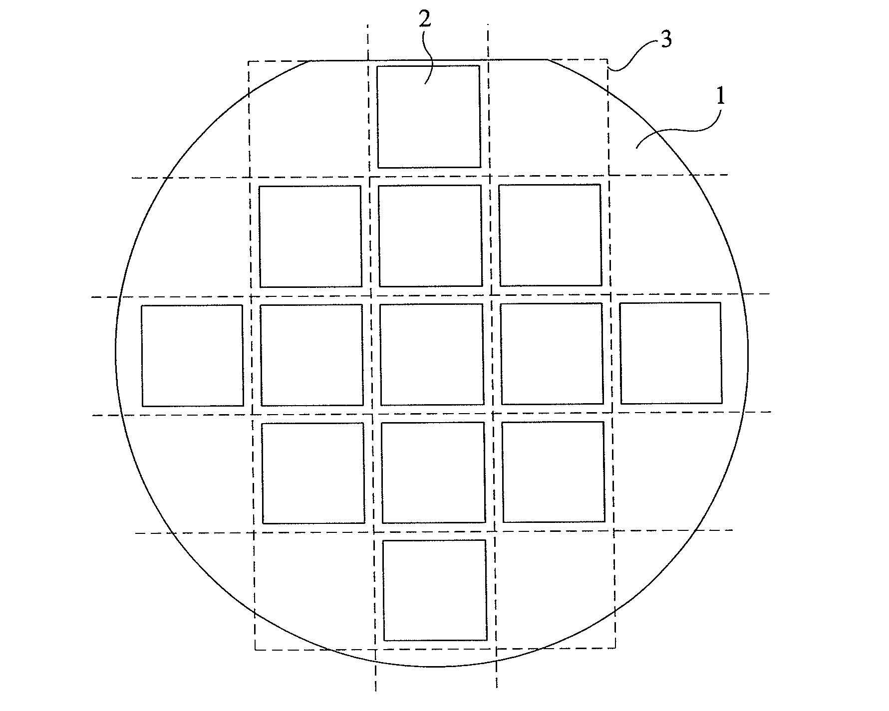
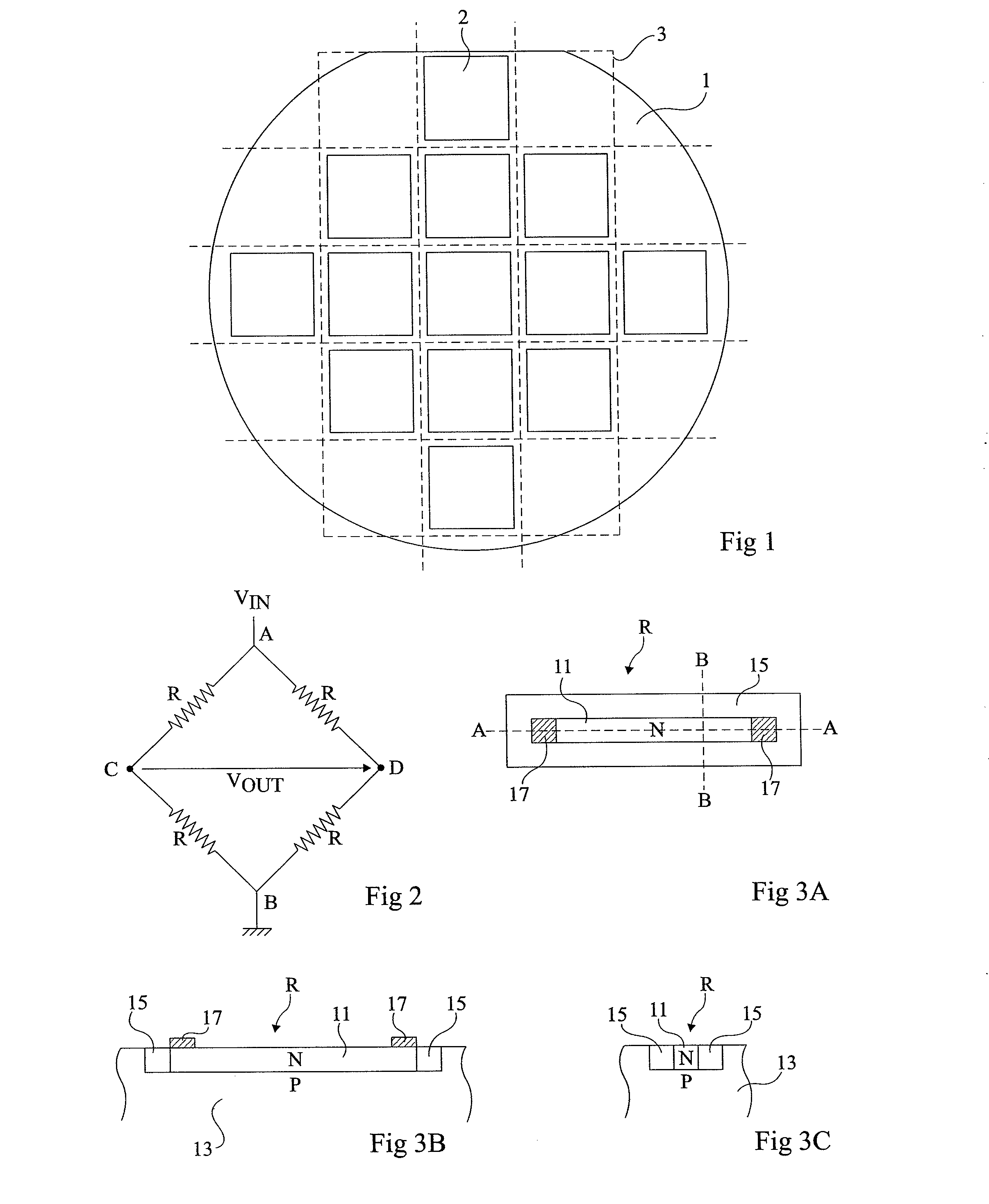
[0026]For clarity, the same elements have been designated with the same reference numerals in the different drawings and, further, as usual in the representation of integrated circuits, the various drawings are not to scale. Only those elements which are necessary to the understanding of the present invention have been shown and will be described hereafter. In particular, the destination and the exploitation made of the generated identifier have not been detailed.

[0027]FIG. 2 shows the electric diagram of a Wheatstone bridge formed of four identical resistors R. A first voltage VIN is applied to a first diagonal of the bridge, between nodes A and B. A possible imbalance voltage VOUT appears on a second diagonal of the bridge, between nodes C and D.

[0028]Since the resistors have the same values, the Wheatstone bridge is normally balanced and output voltage VOUT is equal to 0 V whatever the value of VIN. However, in practice, the resistors are never strictly identical, and the bridge ...


PUM


Abstract

A element for identifying an integrated circuit chip having identical diffused resistors connected as a Wheatstone bridge.

Description

CROSS REFERENCE TO RELATED APPLICATIONS[0001]This application claims the priority benefit of French patent application number 09 / 54056, filed on Jun. 17, 2009, entitled “INTEGRATED CIRCUIT CHIP IDENTIFICATION ELEMENT,” which is hereby incorporated by reference to the maximum extent allowable by law.BACKGROUND OF THE INVENTION[0002]1. Field of the Invention[0003]The present invention generally relates to the identification of integrated circuit chips by means of an identifier which differentiates one chip from another.[0004]2. Discussion of the Related Art[0005]FIG. 1 is a simplified top view of a wafer 1 of a semiconductor material on which circuits or chips 2, all identical, have been formed. Reference will be made to integrated circuit chips, knowing that each chip may comprise one or several active and / or passive circuit(s). Currently, a much higher number of chips than what is shown is formed on a same wafer. At the end of the manufacturing, chips 2 are separated by being cut, f...

Claims


Application Information

Patent Timeline
Patent Type & Authority Applications(United States)
IPC IPC(8): G01R27/08
CPCH01L23/544H01L2223/5444H01L2223/54433H01L27/0802H01L2924/0002H01L2924/00
Inventor FORNARA, PASCALRIVERO, CHRISTIAN
Owner STMICROELECTRONICS (ROUSSET) SAS
Features
  • R&D
  • Intellectual Property
  • Life Sciences
  • Materials
  • Tech Scout
  • Unparalleled Data Quality
  • Higher Quality Content
  • 60% Fewer Hallucinations
Learn More