Semiconductor integrated circuit

a technology of integrated circuits and semiconductors, applied in the direction of multi-input and output pulse circuits, pulse manipulation, pulse techniques, etc., can solve the problems of lowering the yield of products, high cost of testing at actual transfer rate,

Inactive Publication Date: 2011-07-28
KK TOSHIBA
View PDF6 Cites 16 Cited by
  • Summary
  • Abstract
  • Description
  • Claims
  • Application Information

AI Technical Summary

Problems solved by technology

For example, a test at an actual transfer rate using the high speed tester is expensive, and there is a problem in cost.
If the low speed tester is used, t

Method used


Image

  • Semiconductor integrated circuit
  • Semiconductor integrated circuit
  • Semiconductor integrated circuit

Examples


first embodiment

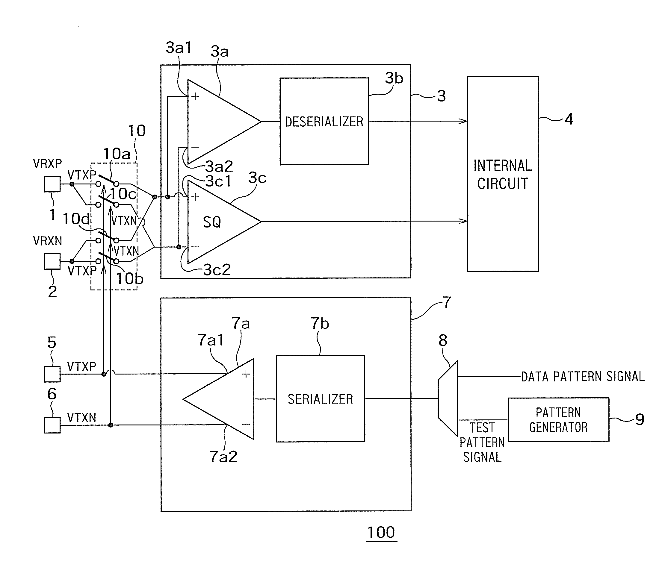
[0024]FIG. 1 is a diagram showing an example of a configuration of a semiconductor integrated circuit 100 according to a first embodiment which is an aspect of the present invention.

[0025]As shown in FIG. 1, the semiconductor integrated circuit 100 includes a first reception terminal 1, a second reception terminal 2, a reception circuit 3, an internal circuit 4, a first transmission terminal 5, a second transmission terminal 6, a transmission circuit 7, a multiplexer 8, a pattern generator 9, and a switch device 10.

[0026]The reception circuit 3 is, for example, a reception line (RX block) of SATA and PCIe, and the first reception terminal 1 and the second reception terminal 2 are input devices to the reception line. The transmission circuit 7 is, for example, a transmission line (TX block) of SATA and PCIe, and the first transmission terminal 5 and the second transmission terminal 6 are output devices from the transmission line.

[0027]The first reception terminal 1 is adapted to be s...

second embodiment

[0078]In the first embodiment, the example in which the squelch circuit is tested by applying DC voltages supplied from the tester to the reception terminals has been described.

[0079]On the other hand, in the present second embodiment, an example in which the squelch circuit is tested by providing a test terminal for testing separately and applying a DC voltage from the tester to the test terminal will be described.

[0080]FIG. 7 is a diagram showing an example of a configuration of a semiconductor integrated circuit 200 according to the second embodiment which is an aspect of the present invention. In FIG. 7, the same characters as those in FIG. 1 denote like components in FIG. 1.

[0081]As shown in FIG. 7, the semiconductor integrated circuit 200 includes a first reception terminal 1, a second reception terminal 2, a reception circuit 3, an internal circuit 4, a first transmission terminal 5, a second transmission terminal 6, a transmission circuit 7, a multiplexer 8, a pattern genera...


PUM


Abstract

A semiconductor integrated circuit has a squelch circuit which has a first noninverting input terminal and a first inverting input terminal, which compares differential amplitude between a signal which is input to the first noninverting input terminal and a signal which is input to the first inverting input terminal with a preset threshold, and which outputs a signal depending upon a result of the comparison. The semiconductor integrated circuit has a first switch circuit between a first reception terminal and the first noninverting input terminal. The semiconductor integrated circuit has a second switch circuit between a second reception terminal and the first inverting input terminal. The semiconductor integrated circuit has a third switch circuit between the first reception terminal and the first inverting input terminal. The semiconductor integrated circuit has a fourth switch circuit between the second reception terminal and the first noninverting input terminal.

Description

CROSS-REFERENCE TO RELATED APPLICATION[0001]This application is based upon and claims the benefit of priority from the prior Japanese Patent Application No. 2010-14406, filed on Jan. 26, 2010, the entire contents of which are incorporated herein by reference.BACKGROUND[0002]1. Field[0003]Embodiments described herein relate generally to a semiconductor integrated circuit including a squelch circuit.[0004]2. Background Art[0005]For example, according to serial STA (SATA: Serial Advanced Technology Attachment) which is communication standards between a computer host and a device, either the host or the device transmits a specific pattern (OOB pattern) to the opposite side, when the host and the device return from a power management state with power dissipation reduced or resetting is conducted.[0006]And the receiving side needs to recognize that the sent pattern signal is the OOB pattern signal. A squelch circuit provided in a semiconductor integrated circuit on the receiving side dete...

Claims


Application Information

Patent Timeline
IPC IPC(8): H03K5/22
CPCH03K5/24
Inventor MATSUDERA, KATSUKI
Owner KK TOSHIBA
Why Eureka
Try Eureka