Methods of Forming Nonvolatile Memory Devices Using Nonselective and Selective Etching Techniques to Define Vertically Stacked Word Lines

a technology of non-volatile memory and etching technique, which is applied in the field of three-dimensional semiconductor devices and methods of forming them, can solve the problems of limited application and limited

Inactive Publication Date: 2012-01-05
SAMSUNG ELECTRONICS CO LTD
View PDF3 Cites 323 Cited by
  • Summary
  • Abstract
  • Description
  • Claims
  • Application Information

AI Technical Summary

Problems solved by technology

However, since high-priced equipment is required for miniaturizing a pattern, although the integration degree of a two-dimensional semiconductor memory device is increased, it is still limited.

Method used


Image

  • Methods of Forming Nonvolatile Memory Devices Using Nonselective and Selective Etching Techniques to Define Vertically Stacked Word Lines
  • Methods of Forming Nonvolatile Memory Devices Using Nonselective and Selective Etching Techniques to Define Vertically Stacked Word Lines
  • Methods of Forming Nonvolatile Memory Devices Using Nonselective and Selective Etching Techniques to Define Vertically Stacked Word Lines

Examples


Embodiment Construction

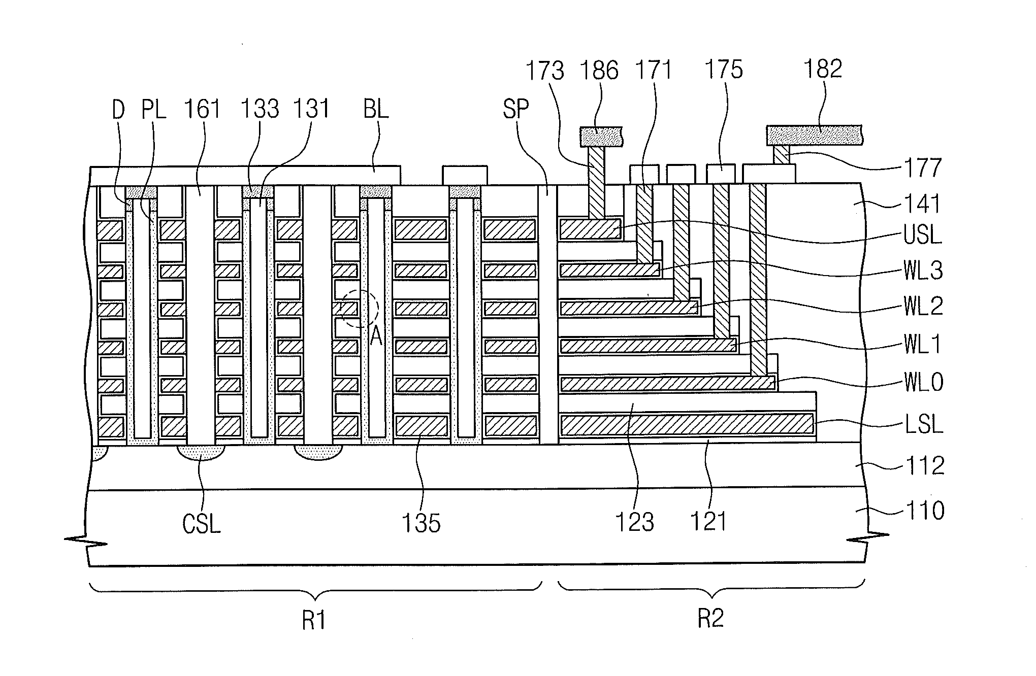
[0043]Exemplary embodiments of the inventive concept will be described below in more detail with reference to the accompanying drawings. The inventive concept may, however, be embodied in different forms and should not be construed as limited to the embodiments set forth herein. Rather, these embodiments are provided so that this disclosure will be thorough and complete, and will fully convey the scope of the inventive concept to those skilled in the art. In the drawings, the dimensions of layers and regions are exaggerated for clarity of illustration. It will also be understood that when a layer (or film) is referred to as being ‘on’ another layer or substrate, it can be directly on the other layer or substrate, or intervening layers may also be present. Further, it will be understood that when a layer is referred to as being ‘under’ another layer, it can be directly under, and one or more intervening layers may also be present. In addition, it will also be understood that when a l...


PUM


Abstract

Methods of forming nonvolatile memory devices include forming a stack of layers of different materials on a substrate. This stack includes a plurality of first layers of a first material and a plurality of second layers of a second material arranged in an alternating sequence of first and second layers. A selected first portion of the stack of layers is isotropically etched for a sufficient duration to define a first trench therein that exposes sidewalls of the alternating sequence of first and second layers. The sidewalls of each of the plurality of first layers are selectively etched relative to sidewalls of adjacent ones of the plurality of second layers. Another etching step is then performed to recess sidewalls of the plurality of second layers and thereby expose portions of upper surfaces of the plurality of first layers. These exposed portions of the upper surfaces of the plurality of first layers, which may act as word lines of a memory device, are displaced laterally relative to each other.

Description

REFERENCE TO PRIORITY APPLICATION[0001]This U.S. non-provisional patent application claims priority under 35 U.S.C. §119 of Korean Patent Application No. 10-2010-0064410, filed on Jul. 5, 2010, the entire contents of which are hereby incorporated by reference.BACKGROUND[0002]The present disclosure relates to semiconductor devices and methods of forming same and, more particularly, to three-dimensional semiconductor devices and methods of forming same.[0003]The increasing degree of integration in semiconductor devices is on demand to satisfy excellent performance and reasonable price. Especially, the degree of integration in a semiconductor memory device is an important factor for determining a product's price. The integration degree of a typical two-dimensional semiconductor memory device is mainly determined by an area that a unit memory cell occupies, so that it is greatly affected by a level of a fine pattern formation technique. However, since high-priced equipment is required f...

Claims


Application Information

Patent Timeline
Patent Type & Authority Applications(United States)
IPC IPC(8): H01L21/8239
CPCH01L27/11551H01L27/11582H01L27/11578H01L27/11556H10B41/50H10B41/20H10B41/27H10B43/50H10B43/20H10B43/27H01L21/67075H01L27/0207H01L27/0688
Inventor KANG, DAEHYUKBAE, SANG WONYOON, BOUNLEE, KUNTACHKIM, YOUNG-HOO
Owner SAMSUNG ELECTRONICS CO LTD
Why Eureka
Try Eureka