Organic light emitting diode display and manufacturing method thereof

a technology of light-emitting diodes and organic light-emitting diodes, which is applied in the direction of basic electric elements, electrical apparatus, and semiconductor devices, can solve the problems of organic light-emitting diodes deteriorating, and achieve the effects of improving the sealing function of the driving circuit portion, reducing the increase of dead space, and improving the use life-span

Active Publication Date: 2012-01-12
SAMSUNG DISPLAY CO LTD
View PDF7 Cites 55 Cited by
  • Summary
  • Abstract
  • Description
  • Claims
  • Application Information

AI Technical Summary

Benefits of technology

[0015]According to the exemplary embodiments, the organic light emitting diode (OLED) display may minimize an increase of dead space and improve a sealing function of the driving circuit portion and the organic light emitting diode by using the thin film encapsulation layer and adhesive layer and absorption functional layer. As a result, a use life-span may be increased and a deterioration of the organic light emitting diode may be minimized.

Problems solved by technology

An organic light emitting diode may deteriorate due to penetration of external moisture, oxygen and ultraviolet (UV) radiation.

Method used


Image

  • Organic light emitting diode display and manufacturing method thereof
  • Organic light emitting diode display and manufacturing method thereof
  • Organic light emitting diode display and manufacturing method thereof

Examples


Embodiment Construction

[0023]Korean Patent Application No. 10-2010-0065571, filed on Jul. 7, 2010, in the Korean Intellectual Property Office, and entitled: “Organic Light Emitting Diode Display and Manufacturing Method Thereof,” is incorporated by reference herein in its entirety.

[0024]Example embodiments will now be described more fully hereinafter with reference to the accompanying drawings; however, they may be embodied in different forms and should not be construed as limited to the embodiments set forth herein. Rather, these embodiments are provided so that this disclosure will be thorough and complete, and will fully convey the scope of the invention to those skilled in the art.

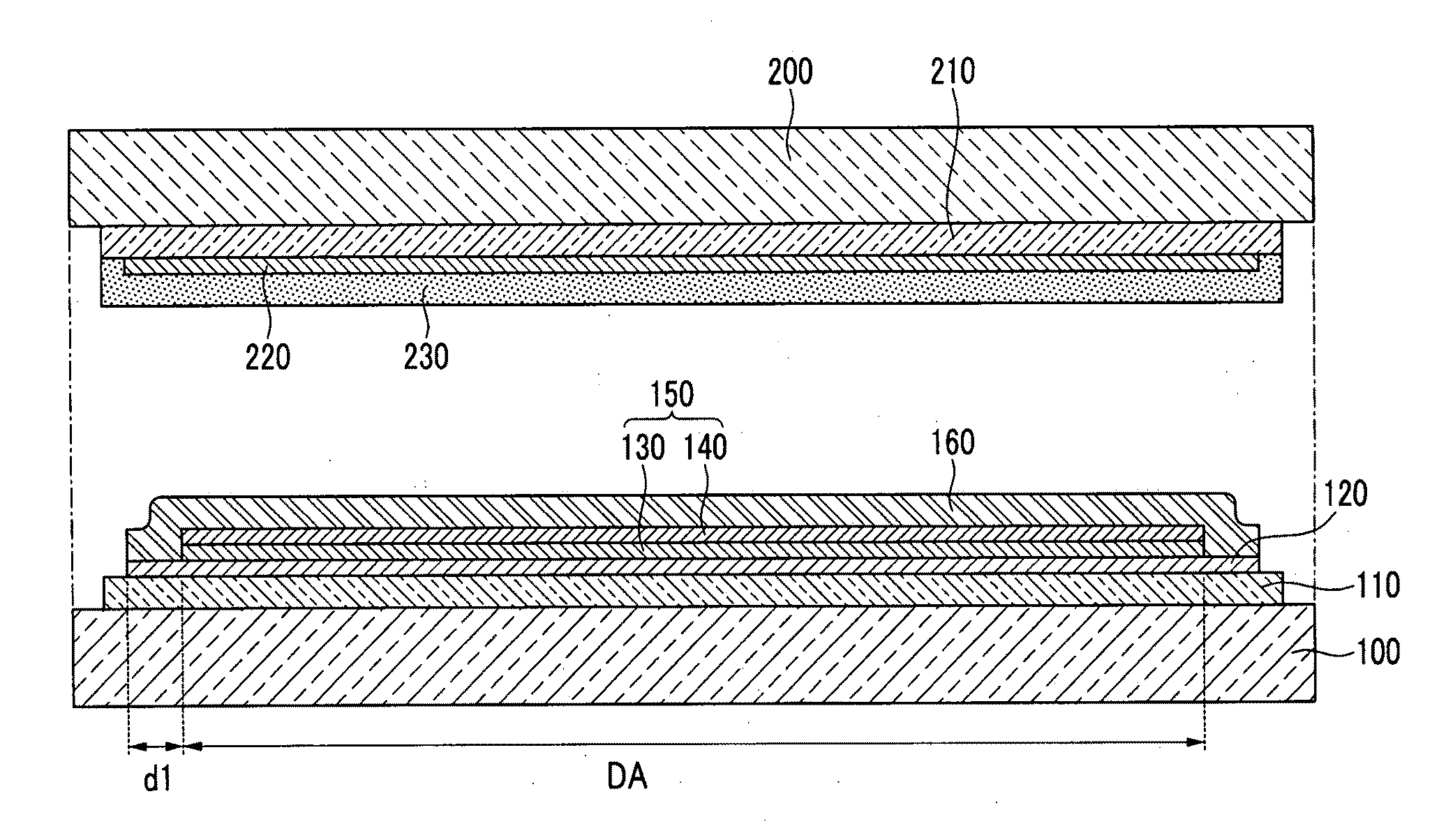
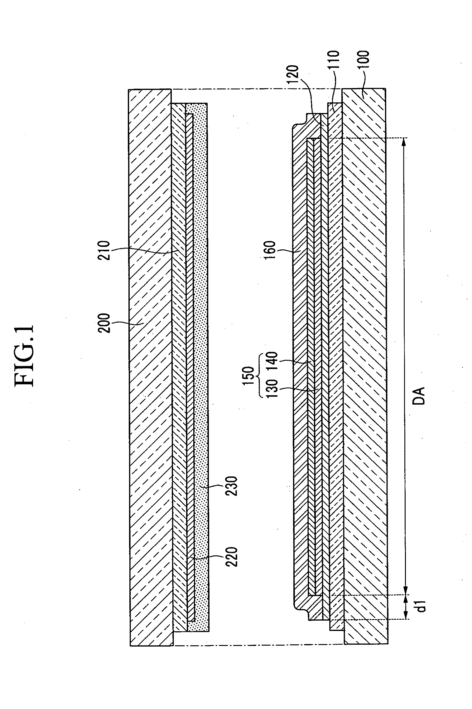
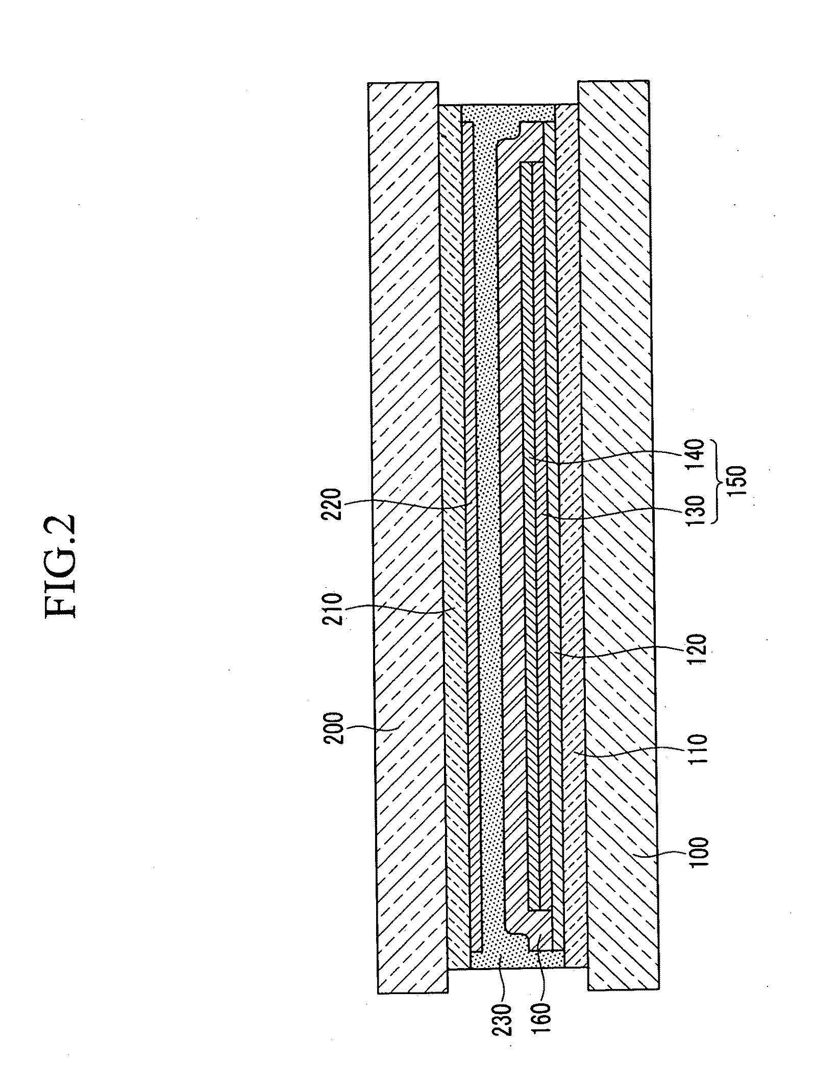
[0025]In the drawing figures, the dimensions of layers and regions may be exaggerated for clarity of illustration. It will also be understood that when a layer or element is referred to as being “on” another layer or substrate, it can be directly on the other layer or substrate, or intervening layers may also be present. Fur...


PUM


Abstract

An organic light emitting diode (OLED) display includes: a first substrate; a display portion that is formed on the first substrate and includes a driving circuit portion and an organic light emitting diode; a thin film encapsulation layer that covers the display portion; an adhesive layer that covers an upper surface and a side of the thin film encapsulation layer; an absorption functional layer that is formed on the adhesive layer and absorbs at least one of oxygen and moisture; and a second substrate that is formed on the absorption functional layer.

Description

BACKGROUND[0001]1. Field[0002]The described technology relates generally to an organic light emitting diode (OLED) display, and more particularly, to an organic light emitting diode (OLED) display to which a thin film encapsulation (TFE) technology is applied and a manufacturing method thereof.[0003]2. Description of the Related Art[0004]An organic light emitting diode (OLED) display is a self light emitting display that is provided with an organic light emitting diode that emits light to display an image. An organic light emitting diode may deteriorate due to penetration of external moisture, oxygen and ultraviolet (UV) radiation.[0005]The above information disclosed in this Background section is only for enhancement of understanding of the background of the described technology and therefore it may contain information that does not form the prior art that is already known in this country to a person of ordinary skill in the art.SUMMARY[0006]An exemplary embodiment provides an orga...

Claims


Application Information

Patent Timeline
Patent Type & Authority Applications(United States)
IPC IPC(8): H01L51/52H01L51/56
CPCH01L51/5259H01L51/5253H10K50/846H10K50/844H10K59/00
Inventor CHOI, JUNG-MI
Owner SAMSUNG DISPLAY CO LTD
Why Eureka
Try Eureka