Data processing apparatus having a flash memory built-in which is rewritable by use of external device
a data processing apparatus and flash memory technology, applied in static storage, digital storage, instruments, etc., can solve problems such as inability to assign processing, and achieve the effect of reducing the chip area of the data processing apparatus
- Summary
- Abstract
- Description
- Claims
- Application Information
AI Technical Summary
Benefits of technology
Problems solved by technology
Method used
Image
Examples
first embodiment
[0076]FIG. 4 is a functional block diagram when the built-in flash memory of the microcomputer MCU1 (which may be formed in a single semiconductor substrate) having the flash memory FMR2, according to the present invention, is subjected to a rewrite processing by a PROM writer.
[0077]FIG. 4 illustrates the central processing unit (hereinafter also referred to merely as “CPU”) 10, the flash memory FMRY2 and the control circuit 20 as exemplary circuit modules sharing the internal bus BUS. This microcomputer MCU1 has a write operation mode by use of the PROM writer 30. For example, when the microcomputer MCU1 is connected to predetermined terminals of the PROM writer 30 through a socket adapter, not shown, the mode setting terminal, not shown, of the microcomputer MCU1 is compulsively set for a predetermined level, so that the operation mode of the microcomputer MCU1 is set for the write mode by the PROM writer 30 (ROM writer write mode operation). In such an operation mode, the CPU 10 ...
second embodiment
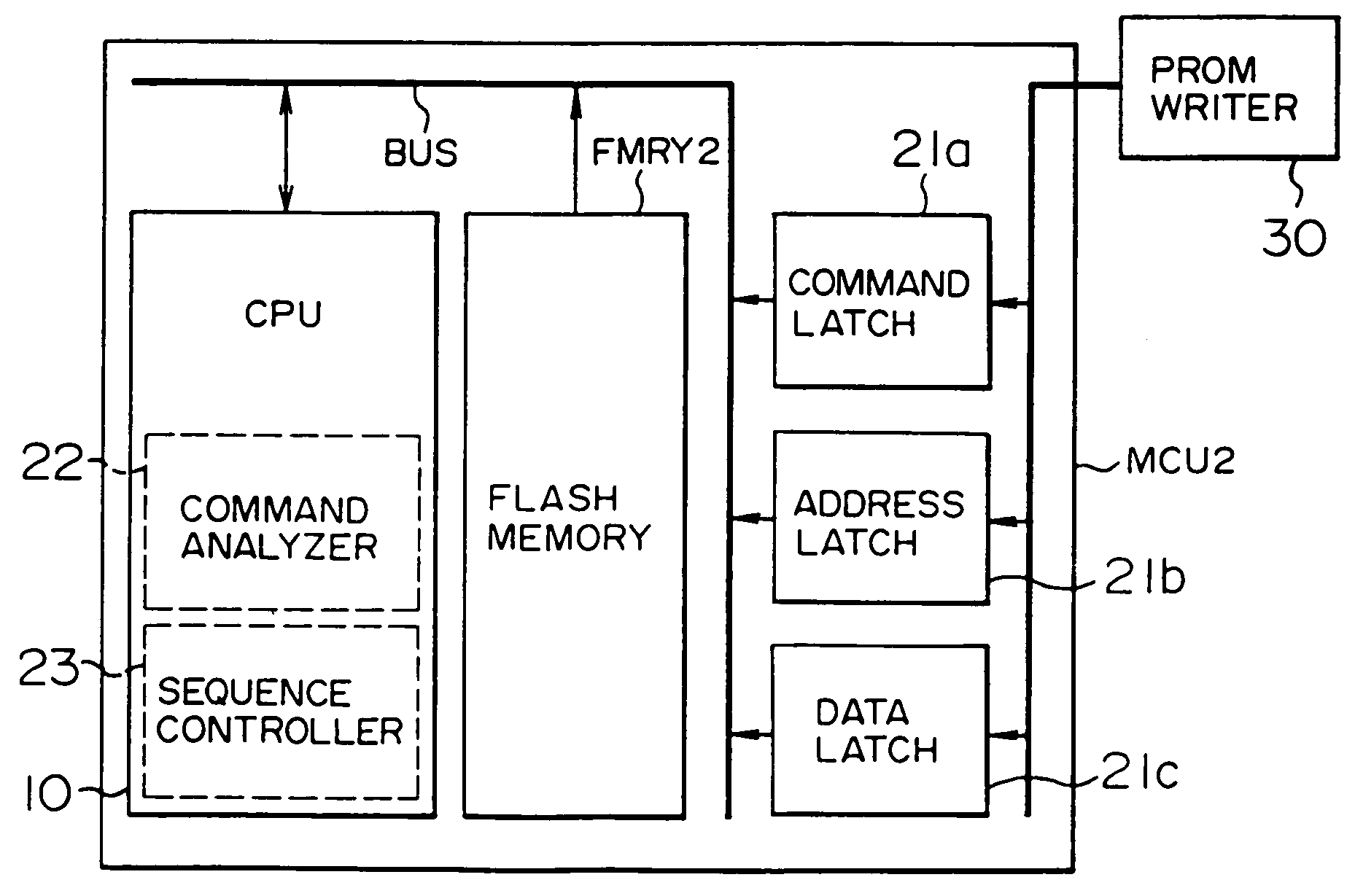
[0079]FIG. 5 shows a functional block diagram of a microcomputer MCU2 (which may be formed in a single semiconductor substrate) having the flash memory FMRY2 built-in in which a rewrite processing is executed for the built-in flash memory MRY2 by the PROM writer 30.
[0080]The microcomputer MCU2 shown in FIG. 5 eliminates the exclusive circuits for rewrite, such as the command analyzer 22 and the sequence controller 23, by allowing the built-in CPU 10 to execute the command analysis and the sequence control without the control circuit 20. In FIG. 5, since the CPU 10 is cut off from the internal bus BUS during the write mode by the PROM writer 30, there is no necessity for the built-in CPU 10 to execute a different processing during the rewrite operation of the flash memory FMRY2 by the PROM writer 30, and therefore, it may be highly possible that the CPU 10 is at halt or dormant, due to the disconnection from the internal bus. The structure shown in FIG. 5 efficiently utilizes such b...
PUM
 Abstract
Description
Claims
Application Information


