Robust ESD LDMOS Device

a metal oxidesemiconductor, robust technology, applied in the direction of semiconductor devices, basic electric elements, electrical equipment, etc., can solve the problem of inferior electrostatic discharging ability of conventional ldmos devices and conventional esd devices, and achieve the effect of improving electrostatic discharging ability and reducing chip area usag

Active Publication Date: 2009-01-08
TAIWAN SEMICON MFG CO LTD
View PDF3 Cites 36 Cited by
  • Summary
  • Abstract
  • Description
  • Claims
  • Application Information

AI Technical Summary

Benefits of technology

[0010]The advantageous features of the present invention include improved electrostatic discharging ability, and reduced chip area usage.

Problems solved by technology

However, the electrostatic discharging ability of conventional LDMOS devices is inferior than conventional ESD devices.

Method used


Image

  • Robust ESD LDMOS Device
  • Robust ESD LDMOS Device
  • Robust ESD LDMOS Device

Examples


Embodiment Construction

[0018]The making and using of the presently preferred embodiments are discussed in detail below. It should be appreciated, however, that the present invention provides many applicable inventive concepts that can be embodied in a wide variety of specific contexts. The specific embodiments discussed are merely illustrative of specific ways to make and use the invention, and do not limit the scope of the invention.

[0019]A lateral diffused metal-oxide-semiconductor (LDMOS) device and methods of forming the same are provided. The variations of the preferred embodiments are then discussed. Throughout the various views and illustrative embodiments of the present invention, like reference numbers are used to designate like elements.

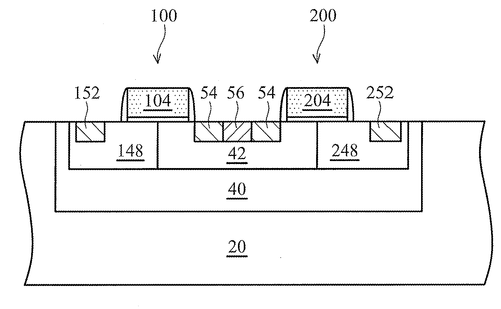
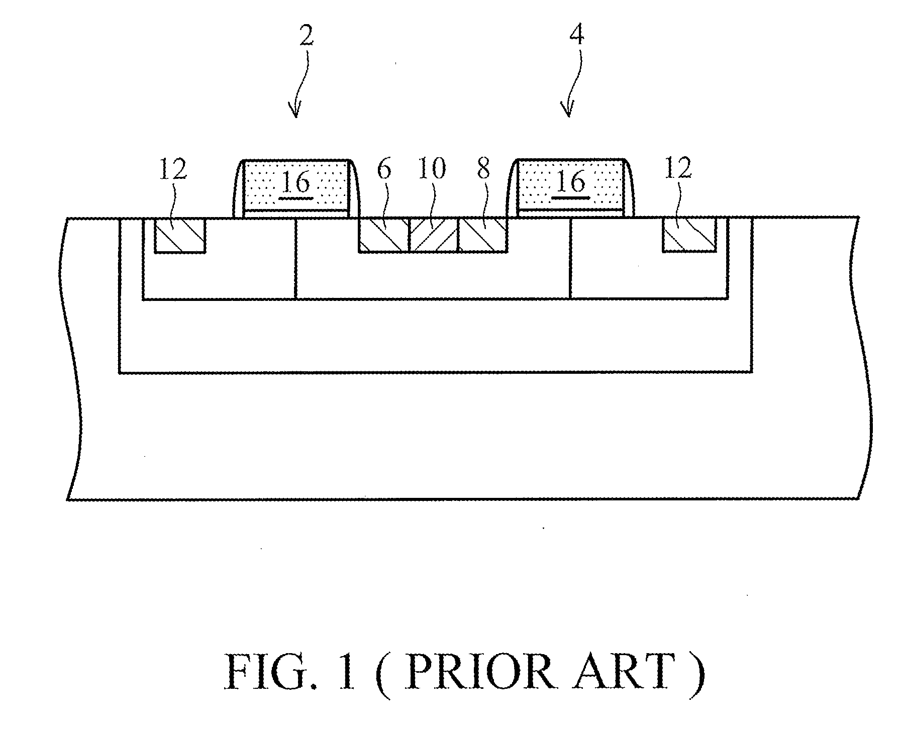
[0020]FIG. 3 illustrates a top view of an embodiment of the present invention. N-type LDMOS (LDNMOS) devices 100 and 200 are formed adjacent to each other, and share common source region 54. Gate 104 of LDNMOS device 100 is connected to gate 204 of LDNMOS device ...


PUM


Abstract

A semiconductor device includes a gate electrode over a semiconductor substrate, wherein the gate electrode has a gate width direction; a source/drain region in the semiconductor substrate and adjacent the gate electrode, wherein the source/drain region has a first width in a direction parallel to the gate width direction; and a bulk pick-up region in the semiconductor substrate and abutting the source/drain region. The bulk pick-up region and the source/drain region have opposite conductivity types. The bulk pick-up region has a second width in the width direction, and wherein the second width is substantially less than the first width.

Description

TECHNICAL FIELD[0001]This invention relates generally to semiconductor devices, and more particularly to structures and formation methods of lateral diffused metal-oxide-semiconductor (LDMOS) devices.BACKGROUND[0002]Lateral diffused metal-oxide-semiconductor (LDMOS) devices are widely used for many types of applications, such as high voltage applications. An LDMOS device typically includes a lightly doped drain region to enhance the breakdown voltage.[0003]FIG. 1 illustrates a cross-sectional view of conventional LDMOS devices 2 and 4, which are formed adjacent to each other, with source regions 6 and 8 therebetween. Heavily doped p-type (P+) bulk pick-up region 10 separates source regions 6 and 8. Drain regions 12 are spaced apart from the respective gate electrodes 16 in order to increase drain-gate voltage. Source regions 6 and 8 and drain regions 12 are doped with an n-type impurity. An LDMOS device may include a plurality of legs connected in parallel, and FIG. 1 illustrates on...

Claims


Application Information

Patent Timeline
Patent Type & Authority Applications(United States)
IPC IPC(8): H01L29/78
CPCH01L29/0696H01L29/7816H01L29/0878
Inventor WEI, CHI-SANWU, KUO-MINGLEE, JIAN-HSING
Owner TAIWAN SEMICON MFG CO LTD
Why Eureka
Try Eureka