Antennas integrated in semiconductor chips

a technology of integrated circuits and semiconductor chips, applied in the field of integrated circuits, can solve the problem of reducing the efficiency of antennas b>4/b>, and achieve the effect of reducing the chip area usage of antennas and improving signal reception

Inactive Publication Date: 2010-07-20
TAIWAN SEMICON MFG CO LTD
View PDF8 Cites 16 Cited by
  • Summary
  • Abstract
  • Description
  • Claims
  • Application Information

AI Technical Summary

Benefits of technology

[0008]The advantageous features of the present invention include reduced chip area usage for antennas and improved reception of signals.

Problems solved by technology

This significantly reduces the efficiency of antenna 4.

Method used


Image

  • Antennas integrated in semiconductor chips
  • Antennas integrated in semiconductor chips
  • Antennas integrated in semiconductor chips

Examples


Embodiment Construction

[0014]The making and using of the presently preferred embodiments are discussed in detail below. It should be appreciated, however, that the present invention provides many applicable inventive concepts that can be embodied in a wide variety of specific contexts. The specific embodiments discussed are merely illustrative of specific ways to make and use the invention, and do not limit the scope of the invention.

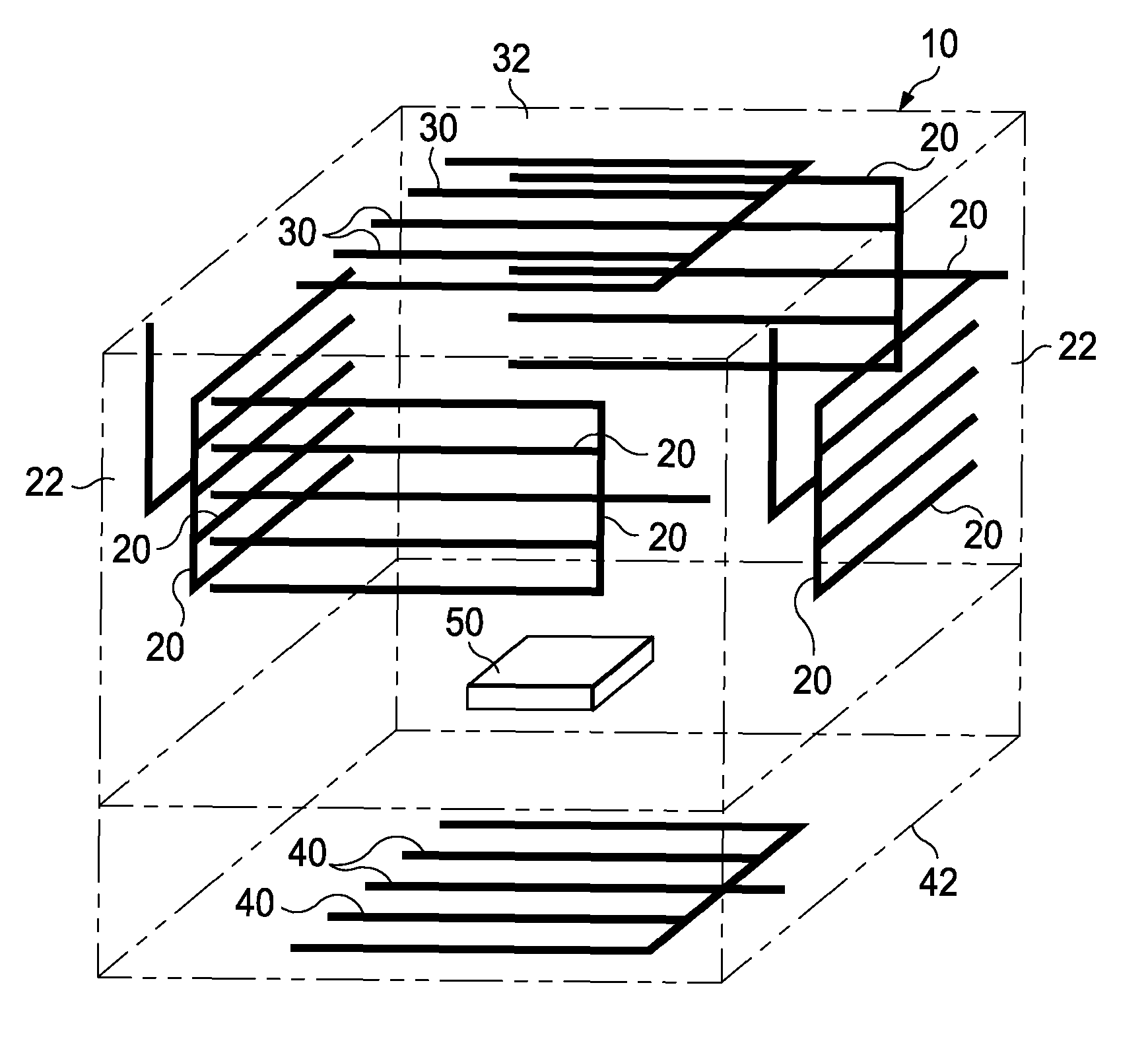
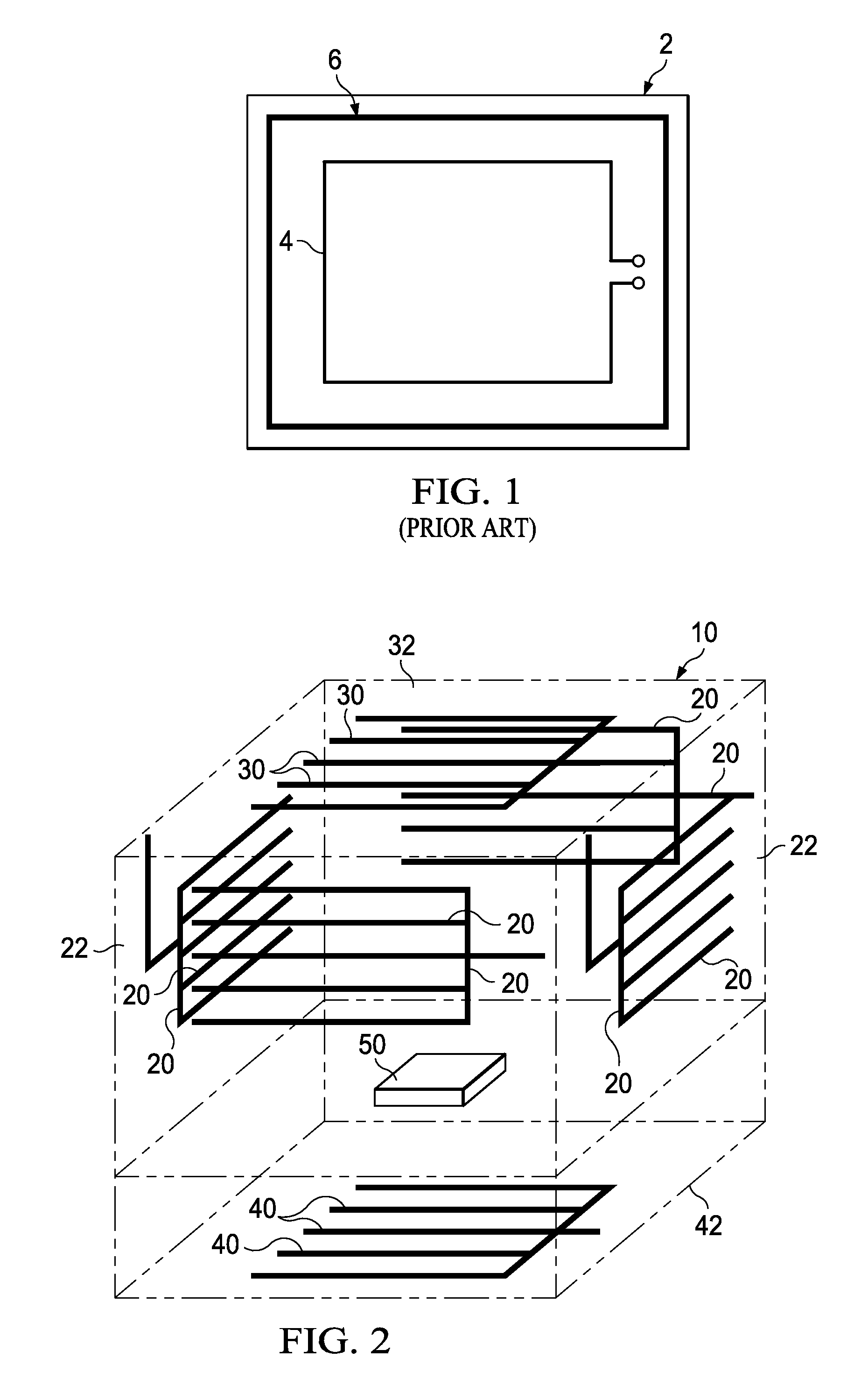
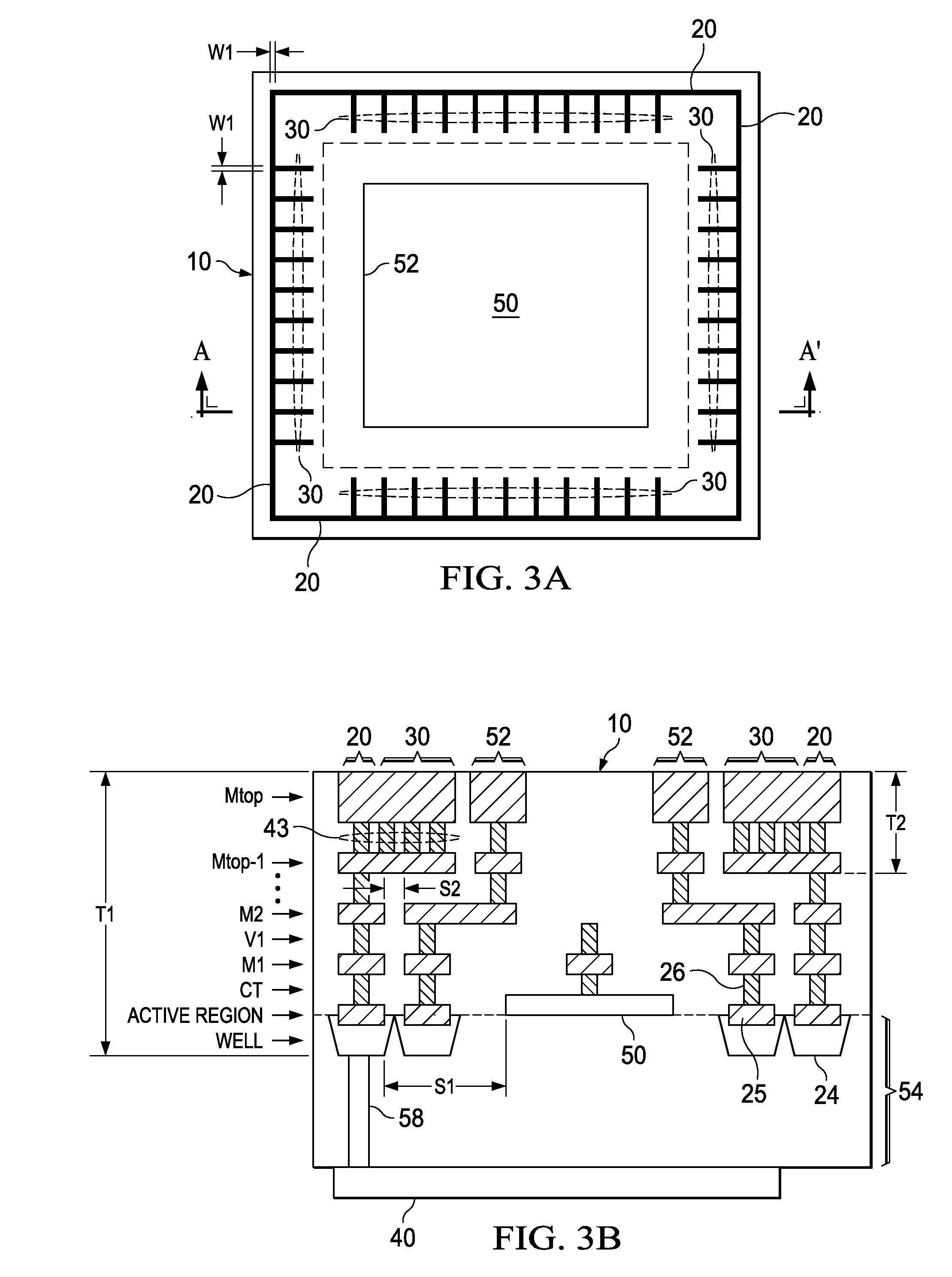
[0015]Novel antennas integrated in semiconductor chips are provided. Throughout the various views and illustrative embodiments of the present invention, like reference numbers are used to designate like elements. It is noted that the figures of the present application may not have accurate scales as in actual semiconductor chips. Particularly, the thicknesses of the semiconductor chips may be exaggerated in order to show vertical structures clearly.

[0016]FIG. 2 illustrates a perspective view of an embodiment of the present invention. Semiconductor chip 10 includes top surface...


PUM


Abstract

An integrated circuit structure includes a semiconductor chip including a top surface, a bottom surface, and a side surface; a metal seal ring adjacent the side surface; and an antenna including a seal-ring antenna. The seal-ring antenna includes at least a portion of the metal seal ring.

Description

TECHNICAL FIELD[0001]This invention relates generally to integrated circuits, and more particularly to antennas integrated in semiconductor chips.BACKGROUND[0002]More and more modern applications require the use of antennas. The applications include wireless communication devices such as mobile phones and other portable devices sending and / or receiving wireless signals. Recently, RFID integrated circuit tags were developed, and are gaining popularity. A common feature of these devices is portability, which demands these devices to be small. Therefore, integrated antennas are formed in the same semiconductor chips as other integrated circuits are developed.[0003]FIG. 1 illustrates a top view of a conventional integrated circuit structure, which includes antenna 4 formed in semiconductor chip 2. The conventional antenna 4, however, suffers from drawbacks. First, partially due to the large area antenna 4 requires, and the spacing required for separating antenna 4 from other integrated ...

Claims


Application Information

Patent Timeline
Patent Type & Authority Patents(United States)
IPC IPC(8): H01Q1/38H01Q1/24
CPCH01L23/585H01L23/66H01L24/48H01L25/0655H01L25/0657H01Q1/38H01Q23/00H01L2223/6677H01L2224/05624H01L2224/05647H01L2224/48091H01L2224/48145H01L2224/48195H01L2224/484H01L2225/06506H01L2924/01013H01L2924/01014H01L2924/01029H01L2924/14H01L2924/19041H01L2924/19042H01L2924/19043H01L2924/00014H01L2924/01005H01L2924/01006H01L2924/01033H01Q1/2283H01L2224/45099H01L2924/00012
Inventor CHANG, CHUNG-LONGLU, DAVID DING-CHUNGCHUNG, SHINE
Owner TAIWAN SEMICON MFG CO LTD
Why Eureka
Try Eureka