Semiconductor storage device and refresh control method therefor

a technology of semiconductors and storage devices, applied in the direction of digital storage, redundant data error correction, instruments, etc., can solve the problems of failure of sorting, inability to improve the efficacy of reducing standby current, etc., to achieve simple structure, prevent the effect of increasing the chip area and preventing the increase of the chip area

Inactive Publication Date: 2005-08-04
LONGITUDE SEMICON S A R L
View PDF5 Cites 36 Cited by
  • Summary
  • Abstract
  • Description
  • Claims
  • Application Information

AI Technical Summary

Benefits of technology

[0034] According to the present invention, the chip area may be prevented from increasing by providing an ECC circuit per bank.
[0035] According to the present invention, the chip area may further be prevented from increasing by providing an error detection circuit of a simpler structure on a bit line between the memory cell array and the sense amplifier.

Problems solved by technology

(B) If the refresh period is sorted with the wafer test (test on a wafer prober), sorting failure occurs if retention time variations occur in a process following the package assembling.
However, if the refresh is carried out frequently, the efficacy in reducing the standby current may not be improved.

Method used


Image

  • Semiconductor storage device and refresh control method therefor
  • Semiconductor storage device and refresh control method therefor
  • Semiconductor storage device and refresh control method therefor

Examples


first embodiment

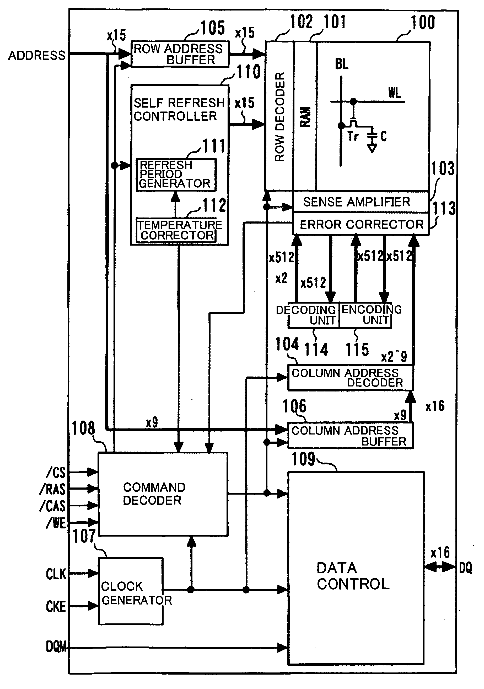
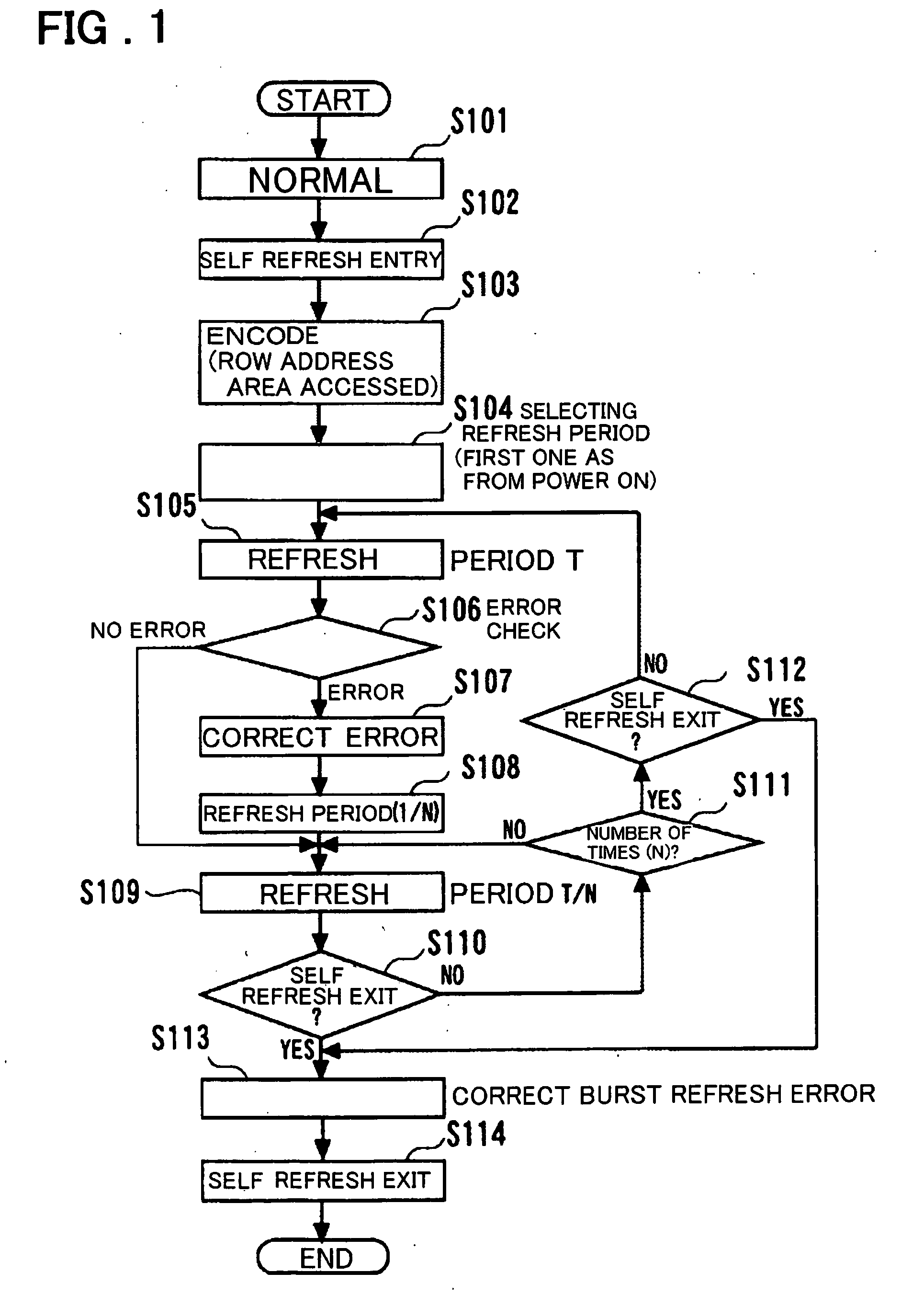
[0066]FIG. 1 illustrates a refresh controlling method according to an embodiment of the present invention. Referring to FIG. 1, the refresh control method according to the present invention is explained. During the normal operation (normal operation mode) of a step S101, the row address accessed is recorded in a storage unit. In self refresh entry of the next step S102, only cell data of the row address area accessed during the normal operation mode is encoded (a check bit by an ECC circuit is generated and stored) (step S103). By limiting the address area for encoding, the current consumption needed in the entry operation to self refresh is decreased. This configuration is one of the main features of the present invention.

[0067] In a step S104, in which the self refresh mode has been entered, the refresh period is selected from one word line to another. That is, the refresh period is selected, preferably at the time of first self refresh entry following power up of the DRAM device....

second embodiment

[0131]FIG. 17 shows the relationship between the current consumption and the inner state during the second cell refresh following power up sequence in the four-valued adaptive refresh in the present invention. Referring to FIG. 17, the first initializing operation following power up sequence of FIG. 16 (selection processing of the refresh period) is omitted and the refresh operation is carried out with the periods of four types of the refresh periods (T / (LMN), T / (MN), T / (N) and T).

[0132]FIG. 18 depicts a table for comparing the Comparative Example (256M-DRAM of the system described in the Patent Publication 2) and the 256M-DRAM of the present embodiment.

[0133] In the present embodiment, the chip size is increased by 7.2%. The increase in the chip size is suppressed to 7.2% by recording, in the DRAM memory cells, the information on the sub-word line SWL based refresh period and the information on the row address accessed during the normal operation.

[0134] In the present embodiment,...


PUM


Abstract

Disclosed is a dynamic semiconductor storage device in which the power supply current during the standby time is diminished to decrease the power consumption and to suppress the chip area from increasing. During the normal operation, the information as to a word line associated with a row address accessed during the normal operation is stored in a RAM. In entering self refresh, data of memory cells connected to a word line associated with a row address accessed during the normal operation time is read out and check bits for the data are appended in an encoder and written in a check bit area. As an initializing operation for the first self refresh entry after power up sequence, the data retention time of the memory cells is inspected every word line. Based on the results of inspection, the setting value of the refresh period of the word line is determined and written in the RAM to set the word line based refresh period. During error check for the refresh operation, any error is corrected by an error correction circuit.

Description

FIELD OF THE INVENTION [0001] This invention relates to a semiconductor storage device and, more particularly, to a dynamic semiconductor storage device having memory cells that are in need of refreshing for data retention, and a refreshing controlling method therefor. BACKGROUND OF THE INVENTION [0002] For reducing current consumption in a dynamic random access memory (DRAM) during the standby time when only data retention is made, it is indispensable to reduce the current during the refresh operation (the operation of amplifying data read out to a bit line from memory cells connected to the word line associated with the refresh address, and of re-storing the read-out data via the bit line). [0003] In the DRAM, where the storage capacity is becoming larger and larger and the miniaturization is advancing, attempts are being made to improve the worst case value of the data retention time of the memory cell by the fabrication process. By way of circuit designing countermeasures, such ...

Claims


Application Information

Patent Timeline
Patent Type & Authority Applications(United States)
IPC IPC(8): G06F11/10G11C7/10G11C11/401G11C11/403G11C11/406
CPCG06F11/1004G11C7/02G11C7/1006G11C7/20G11C11/406G11C11/40615G11C2211/4067G11C11/4072G11C11/4096G11C2207/104G11C2211/4061G11C2211/4062G11C11/40626
Inventor RIHO, YOSHIROITO, YUTAKA
Owner LONGITUDE SEMICON S A R L
Why Eureka
Try Eureka