A novel trench structure power mosfet device and its manufacturing method

A trench and power technology, applied in semiconductor/solid-state device manufacturing, semiconductor devices, electrical components, etc., can solve the problem of unimproved device switching speed and switching loss, reduced device reliability and consistency, limited maximum injection energy, etc. problems, to achieve the effect of increasing the difficulty and cost of process implementation, improving the characteristic on-resistance, and facilitating promotion and mass production

Active Publication Date: 2011-12-14
WUXI NCE POWER
View PDF7 Cites 36 Cited by
  • Summary
  • Abstract
  • Description
  • Claims
  • Application Information

AI Technical Summary

Problems solved by technology

[0005] 1. The P-pillar is formed by multiple high-energy ion implantation methods. Since the ability to inject the maximum energy is determined by the implanter, and the maximum implantation energy of the existing commonly used implanters is relatively limited, the depth of the P-pillar cannot be too large. Deep, for example, boron ions are implanted with 1.5 Mev, and the depth is generally about 3 μm. In this way, the depth of the P column restricts the withstand voltage capability of the device
[0006] 2. Since the device adopts a trench cell structure, the distance between the trenches of adjacent cells is relatively small. Therefore, the lateral injection accompanied by high-energy injection and the final high-temperature pushing junction after injection will affect the trenches on both sides of the P-pillar. The concentration and distribution of P-type impurities near the sidewall of the trench may have a greater impact, which will bring greater risks to the device's turn-on voltage and other parameter characteristics, and reduce the reliability and consistency of the device.
[0007] 3. Like the traditional trench power MOSFET device, the bottom area of ​​the trench is still located in the N-type epitaxial layer. Specifically, the bottom of the gate conductive polysilicon filled in the trench is still located in the N-type epitaxial layer. , and the thickness of the insulating gate oxide layer between the conductive polysilicon and the N-type epitaxial layer is consistent and thin, therefore, when the device is turned on or off, the charging or discharging charge Qgd between the gate and drain is the same as that of the traditional trench power Compared with the Qgd of MOSFET, it has not been significantly improved, so the switching speed and switching loss of the device have not been improved

Method used


Image

  • A novel trench structure power mosfet device and its manufacturing method
  • A novel trench structure power mosfet device and its manufacturing method
  • A novel trench structure power mosfet device and its manufacturing method

Examples


Embodiment Construction

[0065] The present invention will be further described below in conjunction with specific drawings and embodiments.

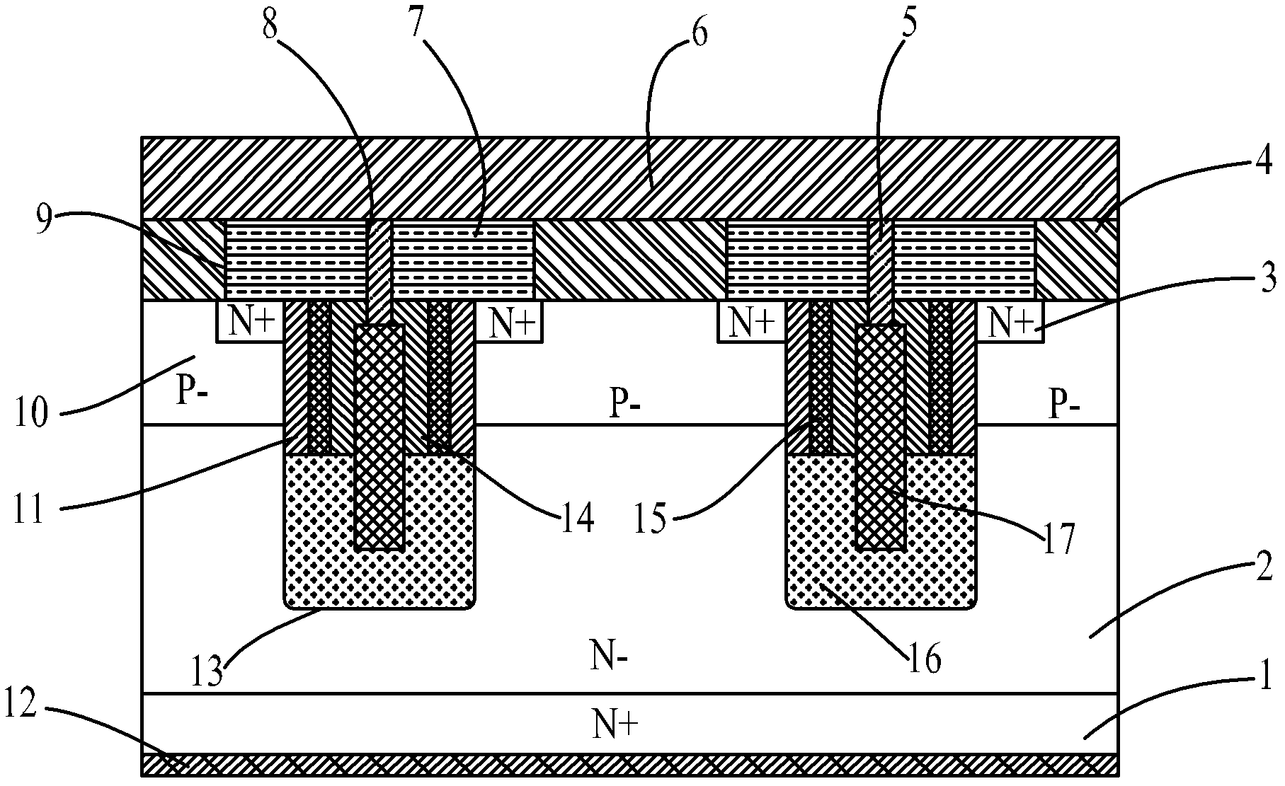
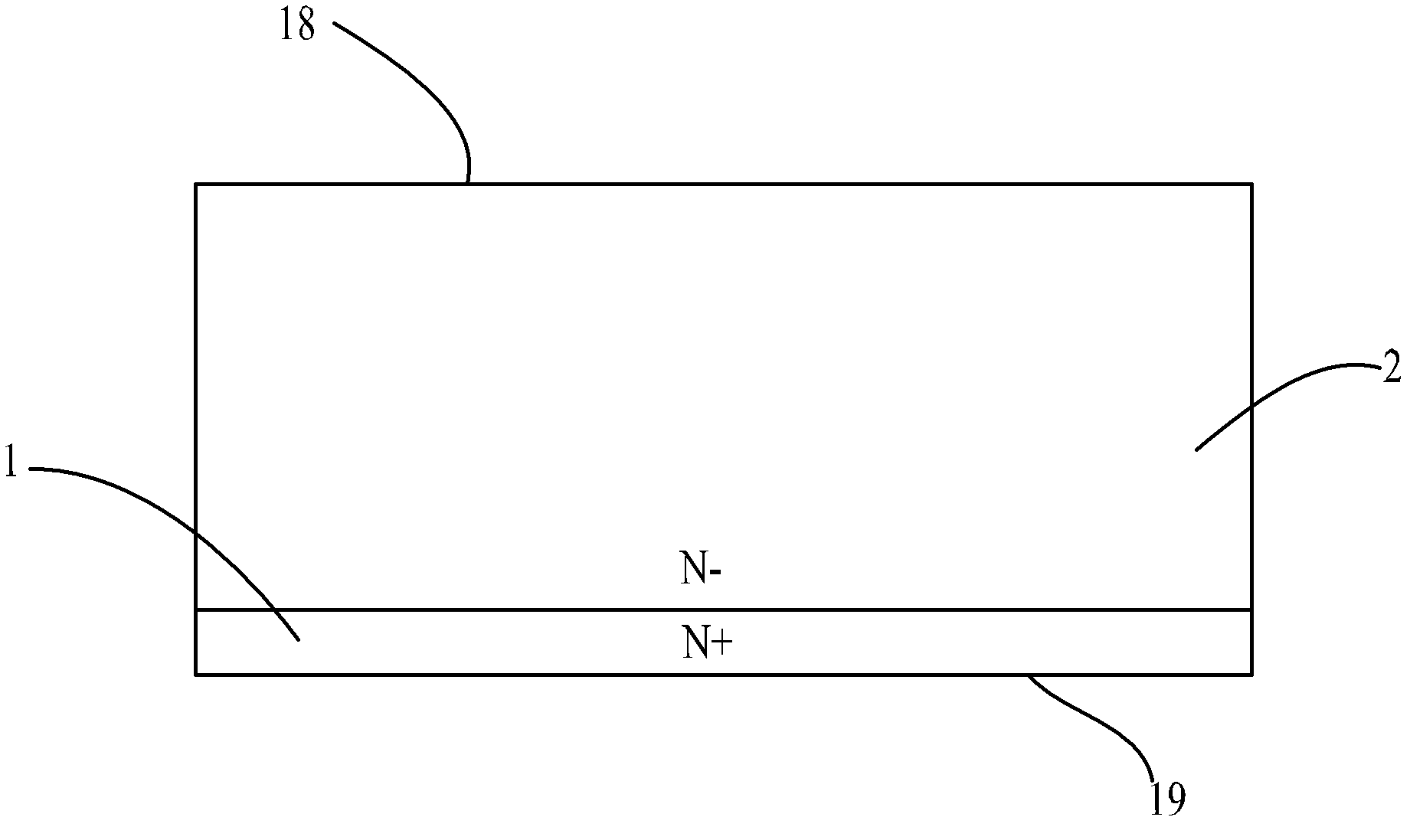
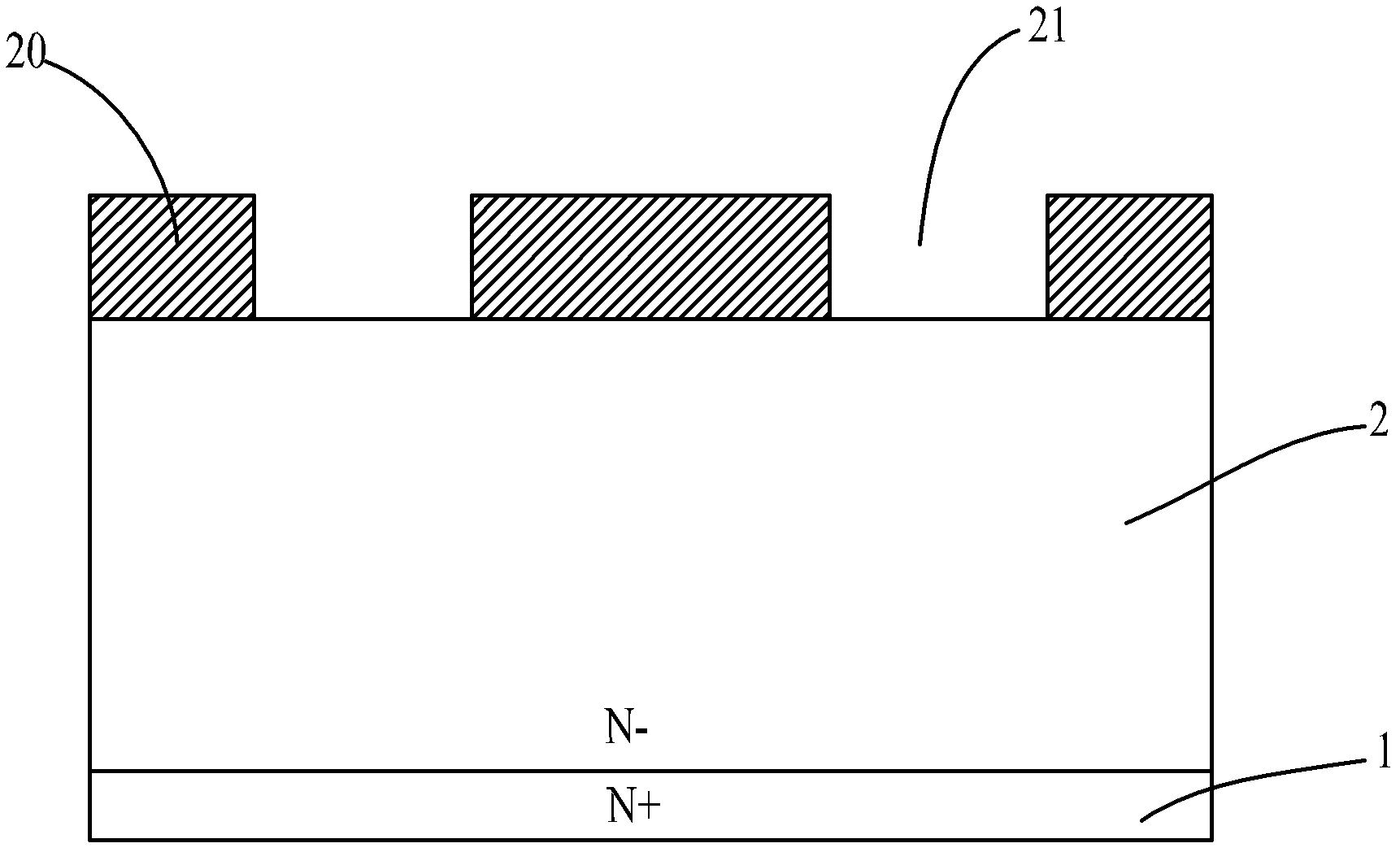
[0066] Such as Figure 1~Figure 16 As shown: taking an N-type power MOSFET device as an example, the present invention includes an N+ substrate 1, an N-type epitaxial layer 2, an N+ injection region 3, a second contact hole filling metal 4, a first contact hole filling metal 5, and a source metal 6. Insulating dielectric layer 7, first contact hole 8, source contact hole 9, P well layer 10, first insulating gate oxide layer 11, drain metal 12, cell trench 13, third insulating gate oxide layer 14 , second conductive polysilicon 15, second insulating gate oxide layer 16, first conductive polysilicon 17, first main surface 18, second main surface 19, hard mask layer 20, hard mask layer window 21, first conductive polysilicon A deposition hole 22 , a first insulating oxide material layer 23 , a first conductive polysilicon material layer 24 , a second insulating o...


PUM


Abstract

The invention relates to a power MOSFET (Metal-Oxide -Semiconductor Field Effect Transistor) device of a novel groove structure and a manufacture method thereof. The unit cell of the element zone of the power MOSFET device adopts groove structure; an insulating oxide layer is arranged in the unit cell groove; the thickness of a second isolated gate oxide layer in the unit cell groove is more thanthe thickness of a first isolated gate oxide layer; conductive polysilicon is deposited in the cell unit groove; the extending distance of the first conductive polysilicon is more than the extending distance of the second conductive polysilicon in the unit cell groove; the groove mouth of the unit cell groove is covered by an insulating medium layer; a source electrode contact hole is filled withsecond contract hole filling metal; the second contract hole filling metal, a first conductive type filling zone and a second conductive type layer are in ohmic contact; source electrode metal is arranged above the unit cell groove; the source electrode metal and the second contact hole filling metal are electrically connected; and the first conductive polysilicon, the source electrode metal and the like are in potential connection. The power MOSFET device has the advantages of low conduction resistance, small grid leak electric charge Qgd, low switching speed, low switching loss, simple technology and low cost.

Description

technical field [0001] The invention relates to a semiconductor device and a manufacturing method thereof, in particular to a novel trench structure power MOSFET device and a manufacturing method thereof, belonging to the technical field of semiconductor devices. Background technique [0002] Super Junction (Super Junction) theory and super junction structure have been widely used in a variety of power MOSFET devices, especially in the 500V to 900V planar power MOSFET device series, which has become the mainstream of this voltage series products, which is mainly Compared with ordinary power MOSFETs, power MOSFETs with super-junction structures have greatly reduced characteristic on-resistance (the product of on-resistance and the area of ​​the active area of ​​the chip) and greatly increased switching speed, thereby reducing the cost of the entire system using this product. power consumption, significantly improving energy efficiency. [0003] The most important condition a...

Claims


Application Information

Patent Timeline
Patent Type & Authority Applications(China)
IPC IPC(8): H01L29/78H01L29/06H01L21/336H01L21/265
CPCH01L29/7813H01L29/407H01L29/66734
Inventor 朱袁正叶鹏丁磊
Owner WUXI NCE POWER
Why Eureka
Try Eureka