
Low voltage, island-layer-based nonvolatile semiconductor storage device with floating biased memory cell channel

a semiconductor storage device and floating bias technology, applied in static indicating devices, instruments, non-linear optics, etc., can solve the problems of inability to reduce the thickness of the gate insulation film, and inability to meet the requirements of low-voltage, so as to reduce the area of the chip, prevent the flow of excessive electric current into the drain, and reduce the width and length of the transistor in the decoder or the booster circuit.

Active Publication Date: 2006-03-07
MASUOKA FUJIO +1
View PDF7 Cites 37 Cited by
  • Summary
  • Abstract
  • Description
  • Claims
  • Application Information

AI Technical Summary

Benefits of technology

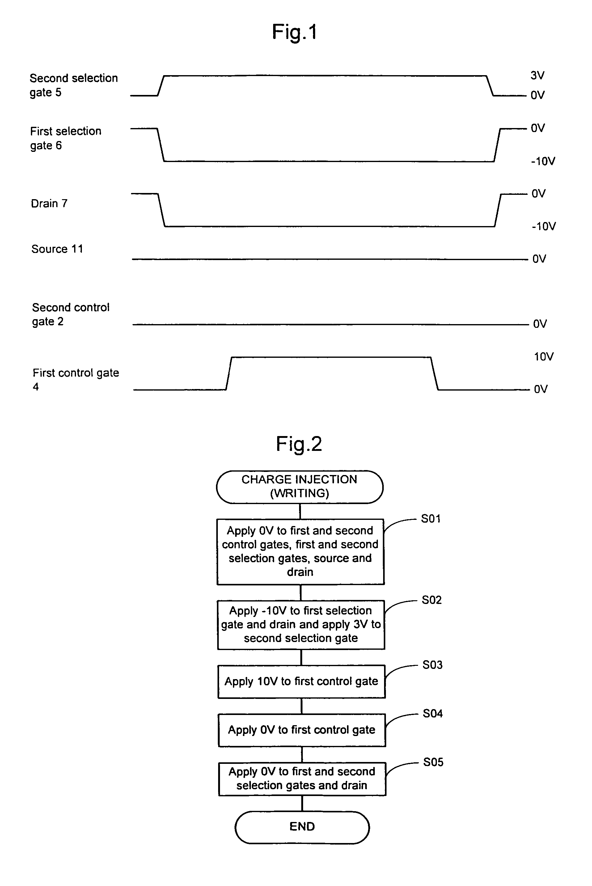
The present invention is about a method for driving a nonvolatile memory device that is less susceptible to the back bias effect. The method reduces the magnitude of the write voltage without complicating the structure of the memory device. The method includes applying a negative voltage to the drain and the first selection gate, while applying a positive voltage to the second selection gate and the control gate of the memory cell for injecting electric charges into the charge storage layer. This prevents excessive electric current flow without the need for a complicated production process and reduces the area of the chip.

Problems solved by technology

Therefore, how to reduce the area of the memory cells and how to increase the capacitance between the floating gate and the control gate are critical issues.
However, the thickness reduction of the gate insulation film has limitation in consideration of the reliability.
However, this approach poses a problem associated with the reliability and, hence, is not practical.
However, this is contradictory to the reduction of the area of the memory cells for the increase of the storage capacity of the nonvolatile memory device.
The back bias effect limits the number of memory cells to be connected in series, thereby hampering the attempt at the increase of the capacitance.
That is, where the back bias effect varies depending on the position on the semiconductor substrate, the threshold voltages of the respective memory cells are liable to be non-uniform.
If the threshold voltages are non-uniform depending on the positions of the memory cells, the write / erase / read voltages for the writing, erasing and reading operations with respect to the memory cells are liable to be non-uniform, resulting in adverse effects such as variations in the characteristics of the memory devices.
In the flash memory cell having the prior art structure, however, the application of the negative voltage to the drain forwardly biases a junction of the P-type semiconductor substrate (ground), resulting in an overcurrent.
Therefore, the simple application of the negative voltage is impractical.
However, this approach is disadvantageous in that the production process is complicated.
Therefore, the simple application of the negative voltage is impractical.
In practice, however, the provision of the triple well structure in a lower portion of the P-type semiconductor layer 12 requires a more complicated production process than the prior art flash memory.

Method used


Image

  • Low voltage, island-layer-based nonvolatile semiconductor storage device with floating biased memory cell channel
  • Low voltage, island-layer-based nonvolatile semiconductor storage device with floating biased memory cell channel
  • Low voltage, island-layer-based nonvolatile semiconductor storage device with floating biased memory cell channel

Examples


first embodiment

[0060]With reference to FIGS. 9 to 28, an explanation will be given to an exemplary production process for producing a nonvolatile memory device of a semiconductor storage device according to the present invention. The nonvolatile memory device to be produced in this embodiment includes an island semiconductor layer formed, for example, by processing a semiconductor substrate into a sea-island configuration and having a peripheral surface serving as an active region, selection transistors provided in association with upper and lower portions of the island semiconductor layer, and a plurality of memory cells (e.g., two memory cells) each including a floating gate including a tunnel oxide film and a charge storage layer provided on the active region of the island semiconductor layer and arranged in series along the island semiconductor layer between the selection transistors. In the nonvolatile memory device, the island semiconductor layer is electrically floated from the semiconducto...

second embodiment

[0074]An exemplary circuit configuration of a semiconductor storage device according to the present invention will be described with reference to FIG. 29. FIG. 29 is a block diagram of the semiconductor storage device 30 according to the invention. The semiconductor storage device 30 includes a plurality of memory cell arrays 31 which each include a plurality of nonvolatile memory devices each including a plurality of memory cells for storing data.

[0075]The memory cell arrays 31 are respectively disposed in blocks B0 to Bn. The blocks B0 to Bn respectively include local row decoders 32B0 to 32Bn. For example, the block B0 includes the local row decoder 32B0. The blocks B0 to Bn each include a plurality of bit lines 51S0 to 51S0i, 51S1 to 51S1i, . . . , 51Sn to 51Sni extending therein, and a plurality of local word lines (not shown) extending therein. The memory cells are respectively disposed at intersections of the local word lines and the bit lines. The bit lines for the respectiv...

third embodiment

[0086]An explanation will be given to a writing operation in which electric charges are injected into a charge storage layer of a nonvolatile memory device according to the present invention.

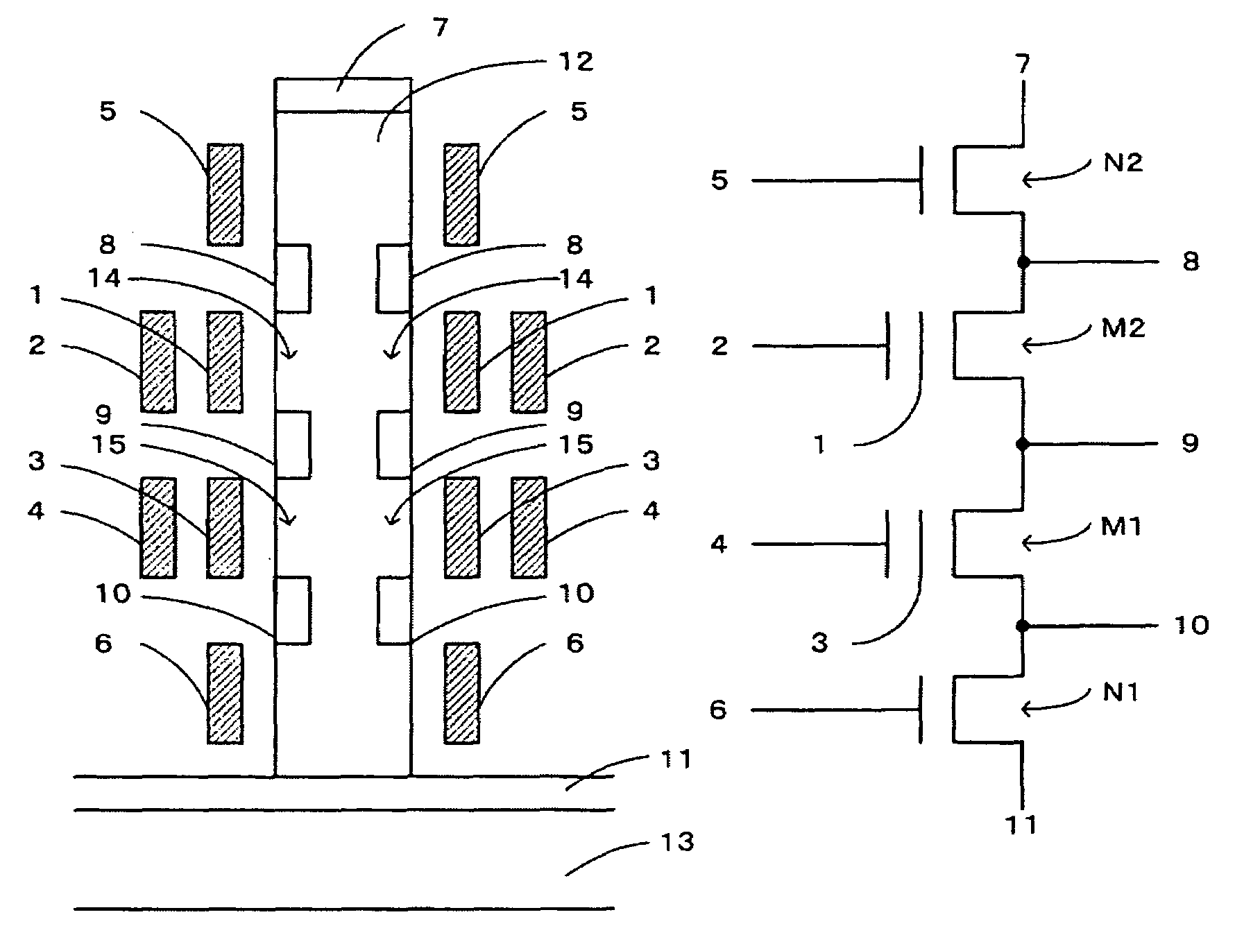
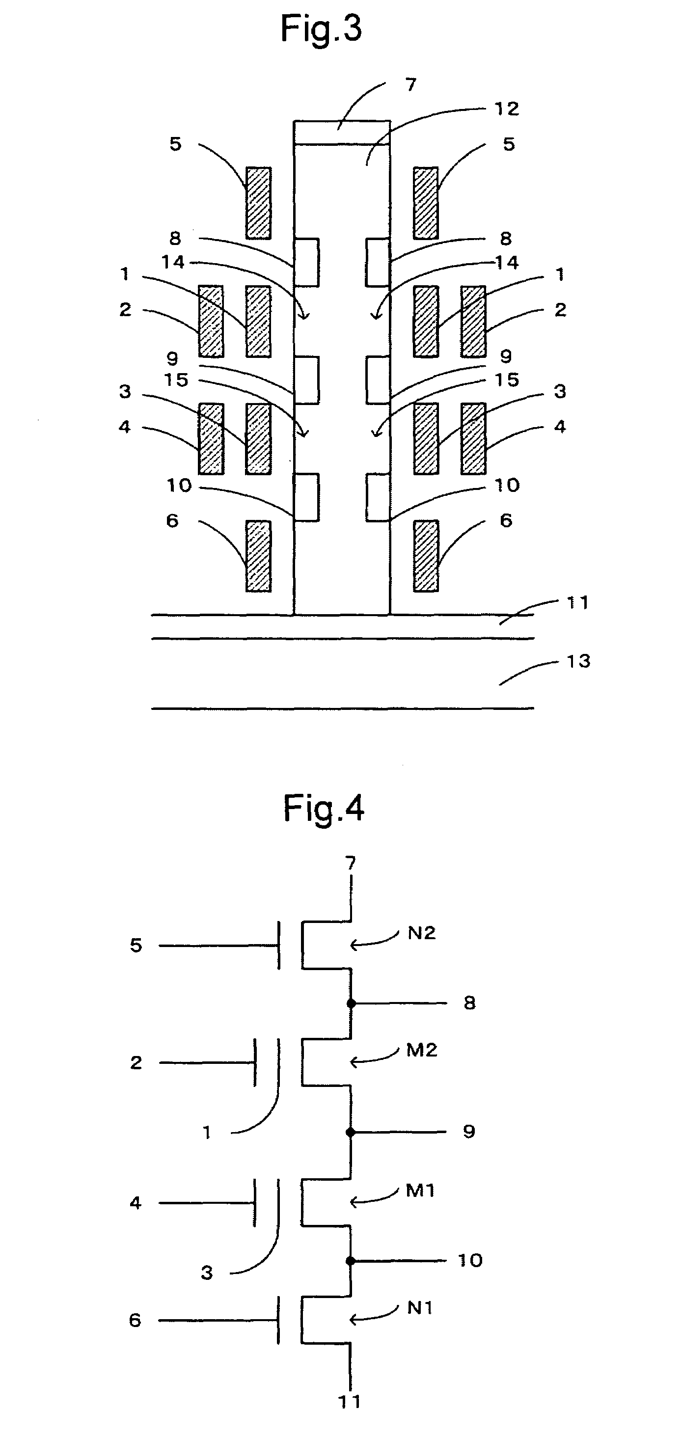
[0087]FIG. 3 is a sectional view of a nonvolatile memory device provided in association with a single island semiconductor layer. FIG. 4 is an equivalent circuit diagram of the nonvolatile memory device, which is equivalent to each of the nonvolatile memory devices constituting the memory cell array shown in FIG. 30. The nonvolatile memory device of FIG. 3 includes two memory cells M1, M2 each having a charge storage layer 1, 3 and a control gate 2, 4 provided around the P-type island semiconductor layer 12 electrically isolated from the P-type semiconductor substrate 13, and two selection transistors N1, N2. An explanation will be given to voltages to be applied to the respective terminals when the electric charges are injected into either of the charge storage layers 1, 3 of the memory cells M...


PUM

PropertyMeasurementUnit
voltageaaaaaaaaaa
read voltageaaaaaaaaaa
thicknessaaaaaaaaaa

Abstract

A method for driving a nonvolatile memory device including a semiconductor substrate, an island semiconductor layer on the substrate, a memory cell having a control gate and a charge storage layer surrounding a peripheral surface of the island semiconductor layer, a first selection transistor provided between the memory cell and the substrate and having a first selection gate, a source diffusion layer between the substrate and the island semiconductor layer, a drain diffusion layer provided in an opposing end of the island semiconductor layer from the source diffusion layer, and a second selection transistor provided between the memory cell and the drain diffusion layer and having a second selection gate, the method comprising the steps of: applying a negative first voltage to the drain and the first selection gate, applying a positive second voltage to the second selection gate, and applying 0V or a positive third voltage to the source; and applying a positive fourth voltage higher than the second voltage to the control gate of the memory cell for injecting electric charges into the charge storage layer.

Description

CROSS-REFERENCE TO RELATED APPLICATION[0001]This application is related to Japanese application No.2003-197409 filed on Jul. 15, 2003 whose priority is claimed under 35 USC §119, the disclosure of which is incorporated by reference in its entirety.BACKGROUND OF THE INVENTION[0002]1. Field of the Invention[0003]The present invention relates to a nonvolatile memory device driving method, a semiconductor storage device, and a liquid crystal display device including the semiconductor storage device.[0004]2. Description of the Related Art[0005]There is known a flash memory whose memory cells each include a control gate and a charge storage layer and have a MOS transistor structure in which electric charges are injected into and released from the charge storage layer by utilizing an FN tunnel current. Data “0” and “1” are stored according to a difference in threshold voltage attributable to a difference in the charge storage state of the charge storage layer. In the case of an N-channel m...

Claims


Application Information

Patent Timeline
Patent Type & Authority Patents(United States)
IPC IPC(8): G11C16/12G02F1/133G02F1/1343G09G3/36G11C16/02G11C16/04G11C16/06G11C16/14G11C16/30H01L21/8247H01L27/10H01L29/788H01L29/792H10B69/00
CPCG11C16/0433H01L29/7887H01L27/115H01L27/11556H01L29/7881G11C16/14G09G3/3611G09G2320/0285H10B41/27H10B69/00G11C16/12G11C16/30H10B41/00
Inventor MASUOKA, FUJIOSAKURABA, HIROSHIMATSUOKA, FUMIYOSHIUENO, SYOUNOSUKEMATSUYAMA, RYUSUKEHORII, SHINJI
Owner MASUOKA FUJIO
Learn More