

Nonvolatile memory device driving method, semiconductor storage device, and liquid crystal display device including the semiconductor storage device
a driving method and non-volatile technology, applied in static indicating devices, instruments, non-linear optics, etc., can solve the problems of inability to achieve the effect of reducing the thickness of the gate insulation film, preventing the flow of excessive electric current into the drain, and reducing the area of the chip
- Summary
- Abstract
- Description
- Claims
- Application Information
AI Technical Summary
Benefits of technology
Problems solved by technology
Method used
Image

Examples
first embodiment
[0060] First Embodiment
[0061] With reference to FIGS. 9 to 28, an explanation will be given to an exemplary production process for producing a nonvolatile memory device of a semiconductor storage device according to the present invention. The nonvolatile memory device to be produced in this embodiment includes an island semiconductor layer formed, for example, by processing a semiconductor substrate into a sea-island configuration and having a peripheral surface serving as an active region, selection transistors provided in association with upper and lower portions of the island semiconductor layer, and a plurality of memory cells (e.g., two memory cells) each including a floating gate including a tunnel oxide film and a charge storage layer provided on the active region of the island semiconductor layer and arranged in series along the island semiconductor layer between the selection transistors. In the nonvolatile memory device, the island semiconductor layer is electrically float...
second embodiment
[0075] Second Embodiment
[0076] An exemplary circuit configuration of a semiconductor storage device according to the present invention will be described with reference to FIG. 29. FIG. 29 is a block diagram of the semiconductor storage device 30 according to the invention. The semiconductor storage device 30 includes a plurality of memory cell arrays 31 which each include a plurality of nonvolatile memory devices each including a plurality of memory cells for storing data.
[0077] The memory cell arrays 31 are respectively disposed in blocks B0 to Bn. The blocks B0 to Bn respectively include local row decoders 32B0 to 32Bn. For example, the block B0 includes the local row decoder 32B0. The blocks B0 to Bn each include a plurality of bit lines 51S0 to 51S0i, 51S1 to 51S1i, . . . , 51S1i to 51Sni extending therein, and a plurality of local word lines (not shown) extending therein. The memory cells are respectively disposed at intersections of the local word lines and the bit lines. The...
third embodiment
[0088] Third Embodiment
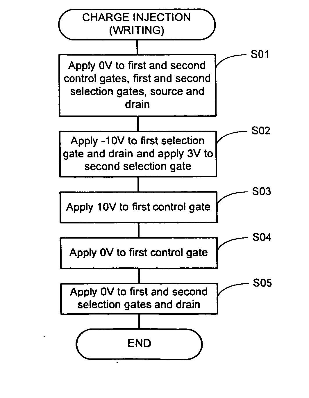
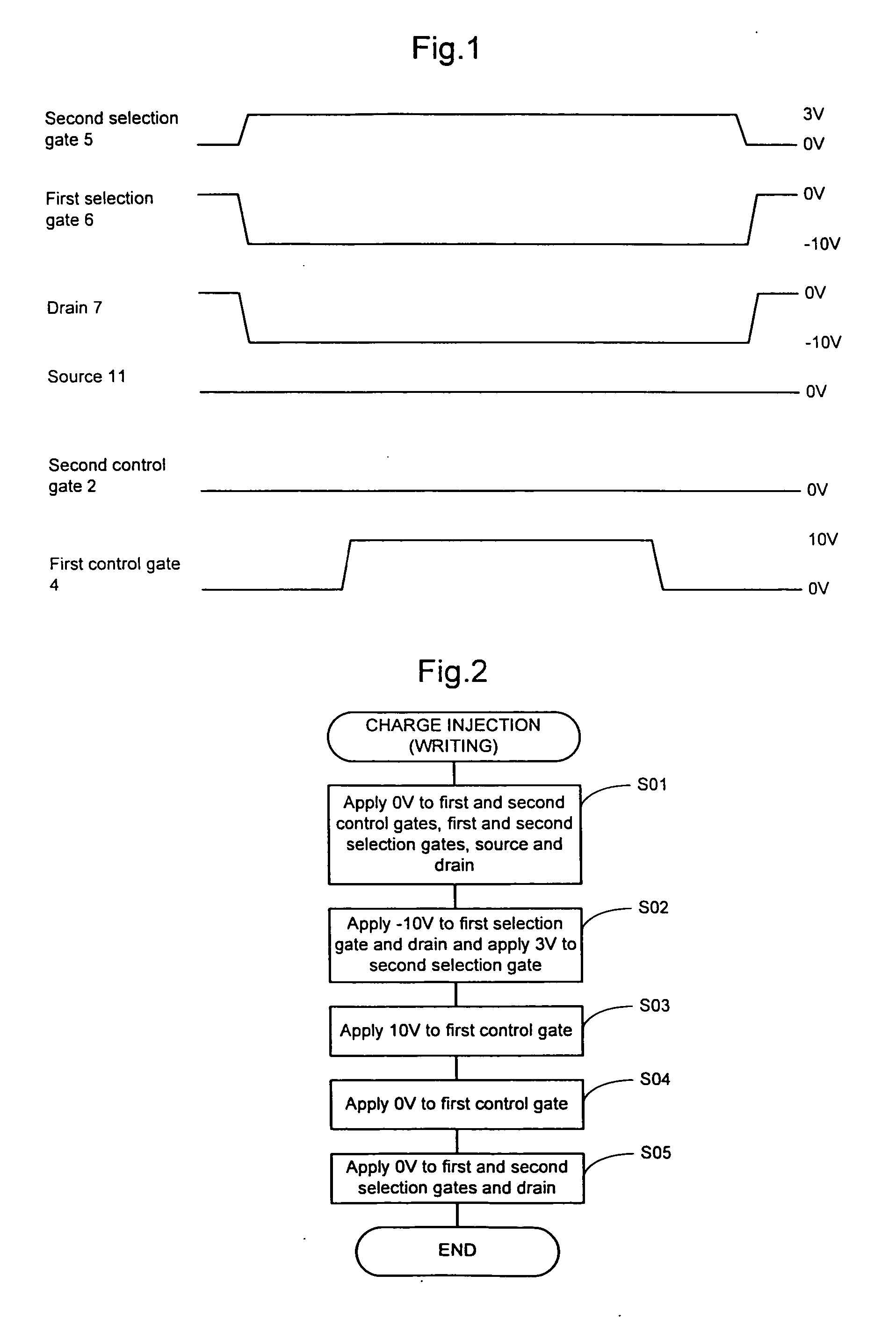
[0089] An explanation will be given to a writing operation in which electric charges are injected into a charge storage layer of a nonvolatile memory device according to the present invention.
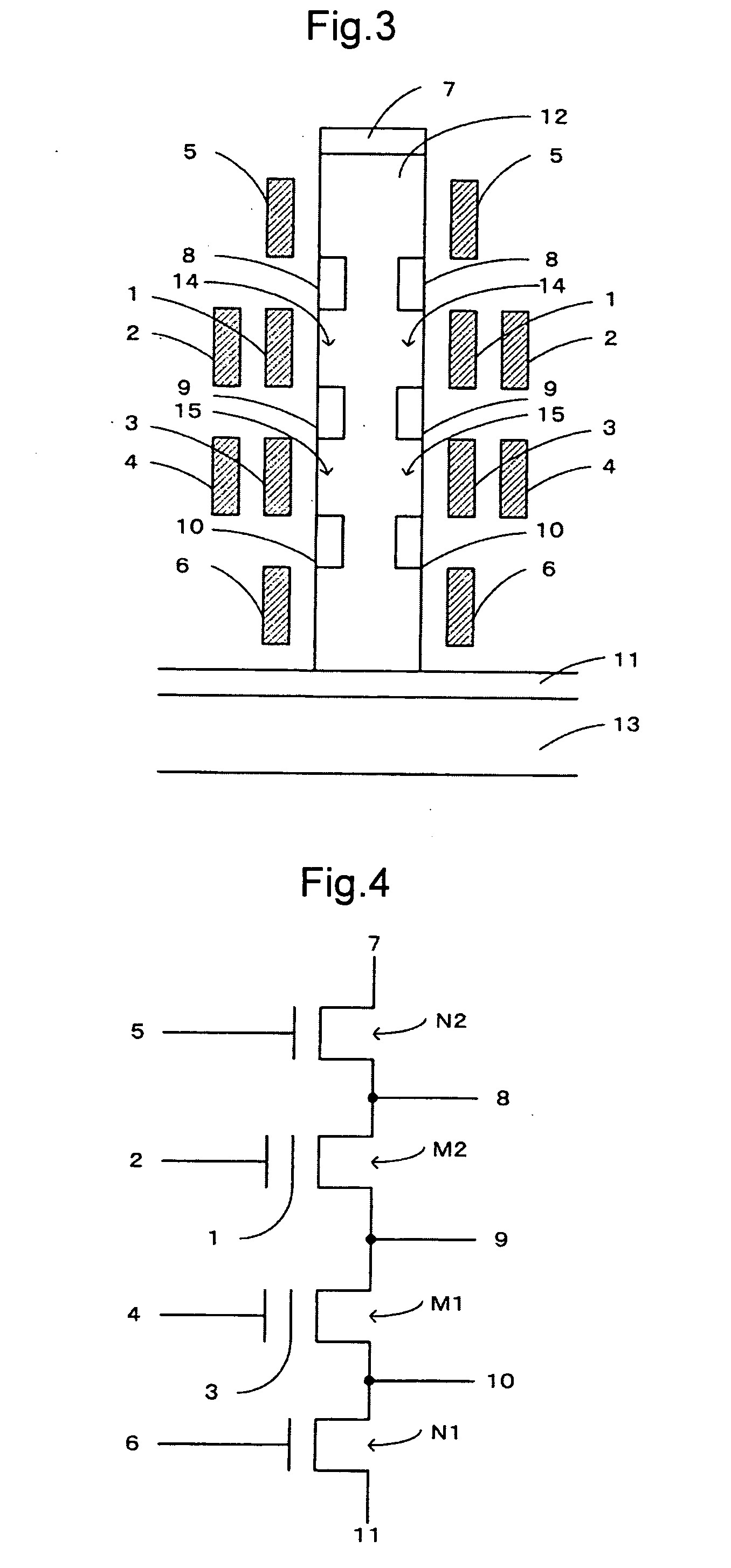
[0090]FIG. 3 is a sectional view of a nonvolatile memory device provided in association with a single island semiconductor layer. FIG. 4 is an equivalent circuit diagram of the nonvolatile memory device, which is equivalent to each of the nonvolatile memory devices constituting the memory cell array shown in FIG. 30. The nonvolatile memory device of FIG. 3 includes two memory cells M1, M2 each having a charge storage layer 1, 3 and a control gate 2, 4 provided around the P-type island semiconductor layer 12 electrically isolated from the P-type semiconductor substrate 13, and two selection transistors N1, N2. An explanation will be given to voltages to be applied to the respective terminals when the electric charges are injected into either of the charge storage layers 1...
PUM
| Property | Measurement | Unit |
|---|---|---|
| voltage | aaaaa | aaaaa |
| read voltage | aaaaa | aaaaa |
| thickness | aaaaa | aaaaa |
Abstract
Description
Claims
Application Information