Low resistance plate line bus architecture

a low-resistance, bus-based technology, applied in the field of memory devices, can solve problems such as particularly likely and problematic situations, and achieve the effects of reducing the resistance of the plate line, reducing the magnitude of negative spikes, and saving chip area

Active Publication Date: 2008-10-28
TEXAS INSTR INC
View PDF5 Cites 22 Cited by
  • Summary
  • Abstract
  • Description
  • Claims
  • Application Information

AI Technical Summary

Benefits of technology

[0020]The invention relates to an improved FeRAM memory array that provides a reduced plate line resistance for arrays having a common plate line connection or a driver. The plate lines that have a common plate line driver are also referred to as plate line group. Use of the common plate line driver for several plate lines is known to save chip area and is commonly used in the current FeRAM circuits. Typically an array of FeRAM with 512 word lines may have 8 or 16 plate groups or drivers. The lower plate line resistance reduces the magnitude of negative spikes on the plate line to reduce the potential for FeCap depolarization. This situation is particularly likely and problematic, for example, when writing a ZERO state to one cell while writing a ONE to many other of the cells on a plate line.
[0021]In accordance with the present invention, the resistance of the plate lines running in a row or word line direction may be lowered by adding one or more plate line interconnections in the column or bit line direction. Two or more plate lines of one or more columns of memory cells are interconnected along the bit line direction. Further, some or all of the plate lines of one or more columns of dummy memory cells may also be interconnected in the bit line direction to reduce the plate line resistance and minimize any increase in the bit line capacitance for the active cells of the array. Thus, the improved FeRAM array provides a reduced data error rate, particularly at fast memory cycle times.
[0023]The array further comprises a plurality of plate lines associated with the rows of memory cells, wherein the plate lines from adjacent cells in a row are arranged adjacent to each other, a common plate line driver connected to, and configured to drive the plurality of plate lines, and first and second memory cells of a first column of memory cells arranged adjacent to each other in a bit line direction. A plate line of the first memory cell is connected to a plate line of the second memory cell, thereby providing a FeRAM memory array having a reduced plate line resistance. The connections between two plate lines in the direction of bit lines is generally referred to as a plate line interconnect or interconnection, or cross-connection.
[0026]In another aspect of the invention, the FeRAM array further comprises some or all of the plate lines of one or more columns of dummy memory cells interconnected along the bit line direction. Beneficially, the use of dummy cells reduces the plate line resistance and minimizes any increase in the bit line capacitance for the active cells of the array.
[0028]In still another aspect of the present invention, two or more adjacent columns of memory cells, comprising several plate lines having a common plate line driver, wherein the adjacent columns each comprise two adjacent memory cells having plate lines interconnected to each other in the bit line direction. Further, each column comprises two more adjacent memory cells having plate lines that are not interconnected to each other in the bit line direction, wherein the interconnections within the columns are offset from one another along the bit line direction. In other words, the plate line interconnections or cross-connections are staggered with respect to each other over the active cells, in order to minimize any increase in the bit line capacitance for the active cells.

Problems solved by technology

This situation is particularly likely and problematic, for example, when writing a ZERO state to one cell while writing a ONE to many other of the cells on a plate line.

Method used


Image

  • Low resistance plate line bus architecture
  • Low resistance plate line bus architecture
  • Low resistance plate line bus architecture

Examples


Embodiment Construction

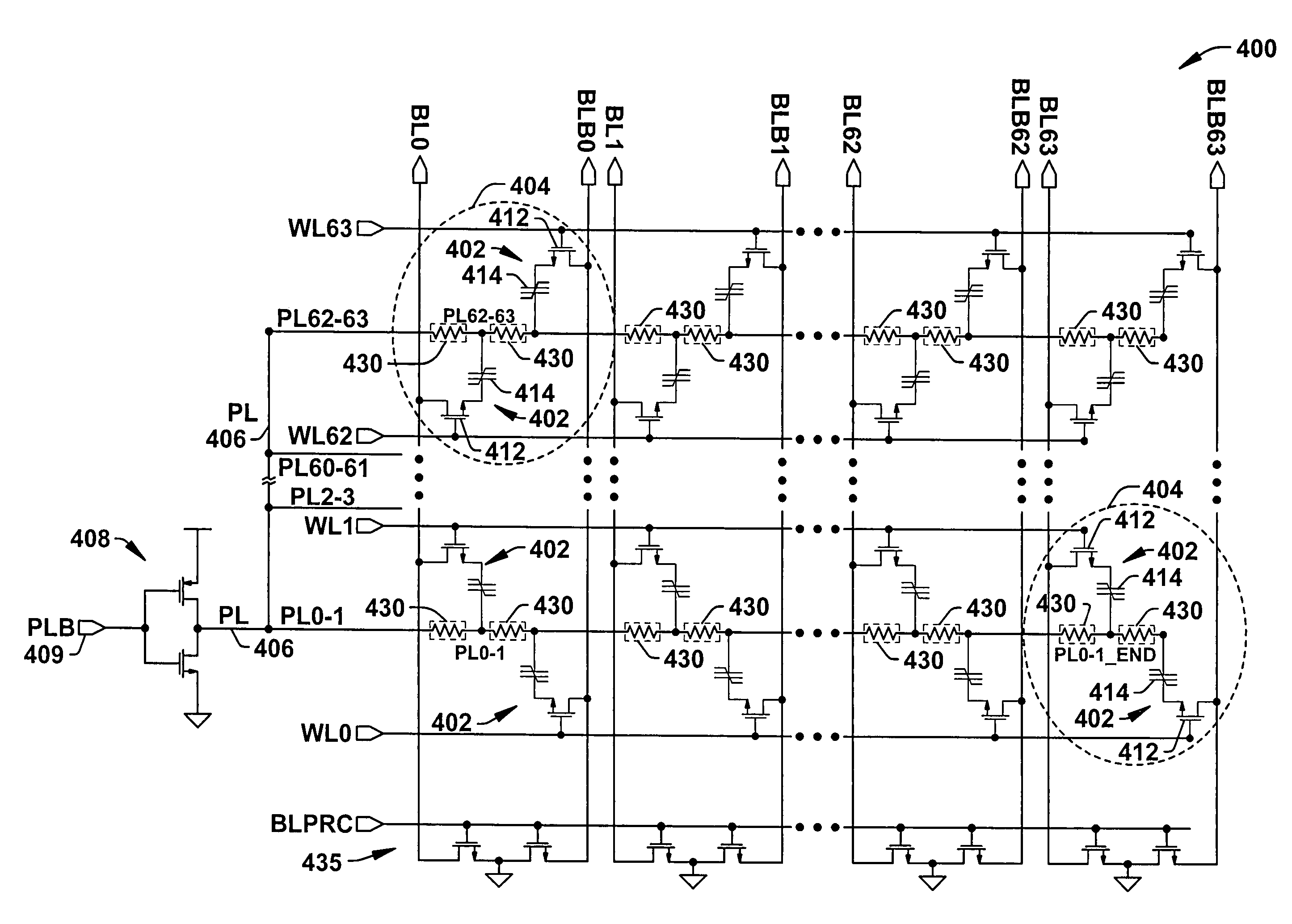
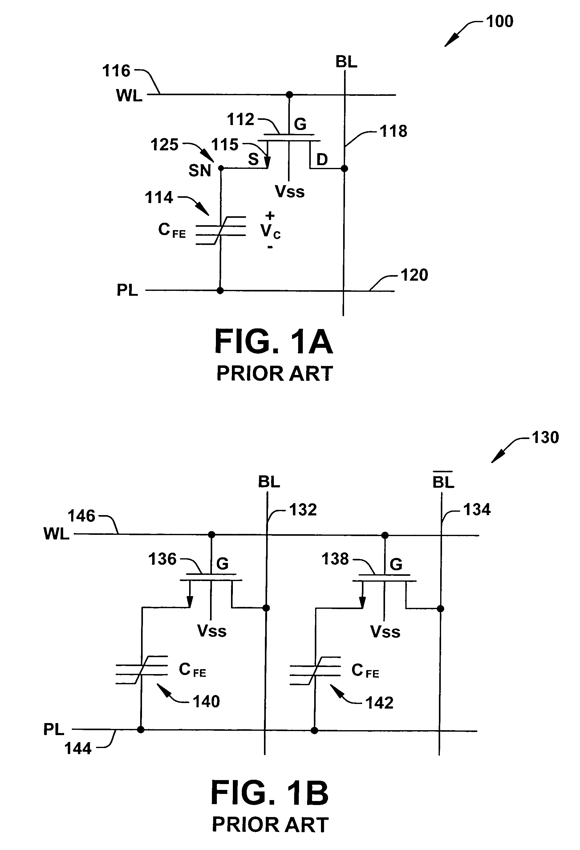
[0041]The present invention will now be described with reference to the attached drawings, wherein like reference numerals are used to refer to like elements throughout. The invention provides an improved FeRAM memory array and other such memory devices having a common plate line connection to provide a reduced plate line resistance. The lower plate line resistance reduces the magnitude of negative spikes on the plate line during write operations to reduce the potential for FeCap depolarization, for example, when writing a ZERO state to one cell while writing a ONE to a significant number of other cells along an associated plate line. The resistance of the plate lines running in a row or word line direction, in accordance with the present invention, may be lowered by adding one or more plate line cross-connections (interconnections) in the column or bit line direction, thereby shorting between the plate lines of adjacent cells of the column. Two or more plate lines of one or more co...


PUM


Abstract

An FeRAM memory array wherein the plate lines run in the direction of word lines is described that provides a reduced plate line resistance in arrays having a common plate line connection. The lower plate line resistance reduces the magnitude of negative spikes on the plate line to reduce the potential for FeCap depolarization. Two or more plate lines of a plurality of columns of memory cells are interconnected along a bit line direction. Some or all of the plate lines of one or more columns of dummy memory cells may also be interconnected to reduce the plate line resistance and minimize any increase in the bit line capacitance for the active cells of the array. The improved FeRAM array provides a reduced data error rate, particularly at fast memory cycle times.

Description

RELATED APPLICATION[0001]This application claims priority to Provisional application No. 60 / 780,613 filed Mar. 9, 2006 entitled A LOW RESISTANCE PLATE LINE BUS ARCHITECTURE.FIELD OF INVENTION[0002]The present invention relates generally to the field of memory devices, and more specifically to a Ferroelectric memory device that provides a reduced plate line resistance in arrays having a common plate line connection, thereby reducing the magnitude of negative spikes on the plate line and the potential for FeCap depolarization.BACKGROUND OF THE INVENTION[0003]Non-volatile ferroelectric RAM, commonly referred to as FeRAM or FRAM devices and other types of semiconductor memories, are used for storing data and / or program code in personal computer systems, embedded processor-based systems, and the like. FeRAM cells employ a ferroelectric capacitor (FeCap) including a pair of capacitor plates with a ferroelectric material, such as SBT or PZT, serving as the capacitor dielectric situated bet...

Claims


Application Information

Patent Timeline
Patent Type & Authority Patents(United States)
IPC IPC(8): G11C11/22
CPCG11C11/22H01L27/11502H10B53/00
Inventor MADAN, SUDHIR KUMARLIN, SUNG-WEIFONG, JOHN
Owner TEXAS INSTR INC
Why Eureka
Try Eureka