Semiconductor integrated communication circuit and operation method thereof

a technology of integrated communication circuit and integrated circuit, which is applied in the direction of dc level restoring means or bias distort correction, transmission monitoring, receiver monitoring, etc., can solve the problems of deterioration, deterioration of second-order distortion characteristic of second-order input intercept point (iip2), and difficulty in resolving the problem of deterioration, so as to minimize the increase in the chip footprint

Inactive Publication Date: 2013-04-02
RENESAS ELECTRONICS CORP
View PDF6 Cites 21 Cited by
  • Summary
  • Abstract
  • Description
  • Claims
  • Application Information

AI Technical Summary

Benefits of technology

[0008]In regard to radio communication terminal devices like mobile phones, it has been required to reduce the number of constituent members from the viewpoint of cost cutting. Especially in recent years, the costs of radio communication terminal devices designed to support WCDMA are kept down by removal of an SAW (Surface-Acoustic-Wave) filter from a receiver. On the other hand, for common receivers for WCDMA, a direct conversion structure has been adopted, because direct-conversion type receivers need fewer circuits and can achieve a reduced power consumption easily as described above. The direct conversion technique is a method by which a receive signal of an RF frequency band is directly converted down to a baseband frequency band. Incidentally, WCDMA is an abbreviation for “Wideband Code-Division Multiple-Access”.
[0013]The method of calibrating an IQ mismatch as disclosed by the patent document JP-A-2008-124965 is based on a method of reducing a receive error (IQ mismatch), which includes the step of supplying a test-signal-generating mixer with a post-division output from a voltage-control oscillator for transmission, and a post-division output from voltage-control oscillator for a digital interface, thereby causing the test-signal-generating mixer to output an RF test signal consisting of a one-tone signal of RF receive frequency band.
[0016]Therefore, it is an object of the invention to provide a semiconductor integrated communication circuit which can minimize the increase in the chip footprint of a test-signal-generating circuit for calibrating both of the second-order input intercept point (IIP2) and IQ mismatch.
[0017]It is another object of the invention to shorten both of the time required for calibration of the second-order input intercept point (IIP2) and the time required for calibration of IQ mismatch.
[0026]It is the invention can provide a semiconductor integrated communication circuit which can minimize the increase in the chip footprint of a test-signal-generating circuit for calibrating both of the second-order input intercept point (IIP2) and IQ mismatch.

Problems solved by technology

At that time, if the second-order distortion characteristic of the receive mixer is bad, a component of second-order intermodulation (IM2) will overlap a receive baseband signal near DC, and thus degrade the sensitivity of signal receive.
The second-order distortion characteristic of the second-order input intercept point (IIP2) is deteriorated owing to the unevenness of the mixers forming a differential pair in a mixer circuit.
Only eliminating the unevenness in manufacturing of integrated circuits, and changing the chip layout thereof, it is still difficult to remedy the problem of the deterioration.
While there are various causes of the receiver noise, the noise coming from a local oscillator is dominant.

Method used


Image

  • Semiconductor integrated communication circuit and operation method thereof
  • Semiconductor integrated communication circuit and operation method thereof
  • Semiconductor integrated communication circuit and operation method thereof

Examples


first embodiment

[0101]>

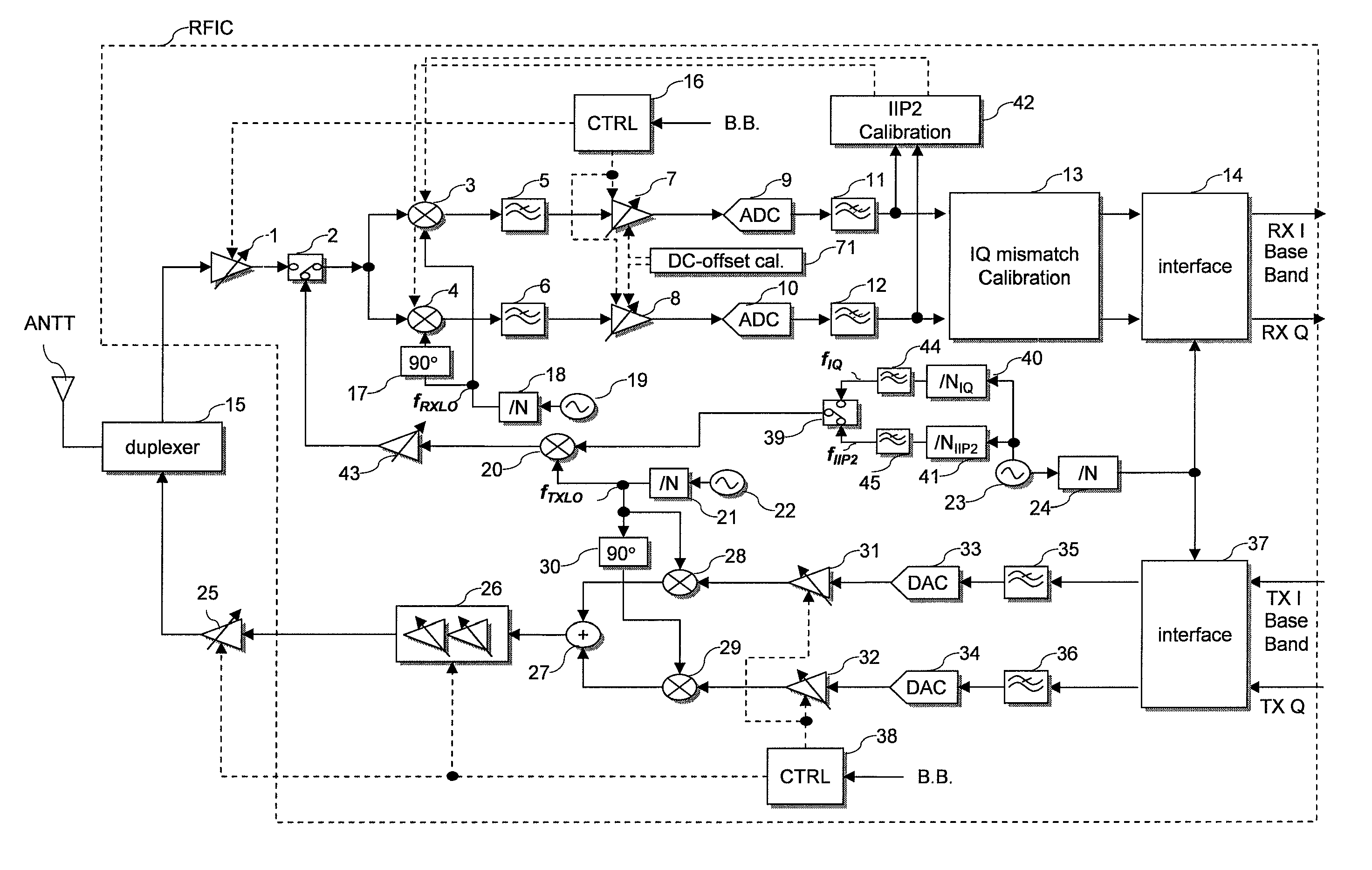
[0102]FIG. 1 is a diagram showing a structure of a radio-frequency semiconductor integrated circuit (RFIC) according to the first embodiment of the invention.

[0103]For RFIC according to an embodiment of the invention, receive-SAW-filter-less, direct-conversion type transmitter-receiver pursuant to UMTS standard are adopted. Now, it is noted that UMTS stands for Universal Mobile Telecommunications System.

[0104]The receiver of RFIC shown in FIG. 1 is composed of a direct conversion type receiver (DCR) having a function for calibrating the second-order input intercept point (IIP2), and a function for calibrating IQ mismatch.

[0105]A mobile phone terminal device with RFIC mounted therein shown in FIG. 1 includes: an antenna ANTT; a low-noise amplifier (LNA) 1; switches 2 and 39; a pair of receive mixers 3 and 4; a test-signal-generating mixer 20; a pair of transmit mixers 28 and 29; low-pass filters (LPF) 5, 6, 11, 12, 35, 36, 44 and 45; variable-gain amplifiers (PGA) 7, 8, 26, 31...

second embodiment

[0202]FIG. 20 is a diagram showing the structure of a radio-frequency semiconductor integrated circuit (RFIC) according to the second embodiment of the invention.

[0203]The difference between RFIC according to the second embodiment of the invention shown in FIG. 20, and RFIC according to the first embodiment of the invention shown in FIG. 1 is as follows.

[0204]In RFIC shown FIG. 1, an oscillating output signal which the digital-interface-voltage-control oscillator (VCO) 23 generates is supplied to input terminals of the divider 41 used in IIP2 calibration mode. However, in RFIC shown in FIG. 20, an oscillating output signal which a reference-signal source 51 outputs through output terminals thereof is supplied to the input terminals of the divider 41 used in IIP2 calibration mode.

[0205]The oscillating output signal from the reference-signal source 51 is divided by the divider 41, whereby a clock signal having the frequency fIIP2 is produced. The clock signal of the frequency fIIP2 is...

third embodiment

[0207]FIG. 21 is a diagram showing the structure of a radio-frequency semiconductor integrated circuit (RFIC) according to the third embodiment of the invention.

[0208]The difference between RFIC according to the third embodiment of the invention shown in FIG. 21, and RFIC according to the first embodiment of the invention shown in FIG. 1 is as follows.

[0209]In RFIC shown FIG. 1, an oscillating output signal which the digital-interface-voltage-control oscillator (VCO) 23 generates is supplied to the input terminals of the divider 41 used in IIP2 calibration mode. However, in RFIC shown in FIG. 21, the digital-to-analog converter (DAC) 52 and digital sine-wave signal source 53 are connected to the input terminals of the divider 41 used in IIP2 calibration mode.

[0210]In the calibrating operation in “IIP2 calibration mode”, digital sine wave data generated by the digital sine-wave signal source 53 is supplied to the digital-to-analog converter 52. In response to it, the digital-to-analo...


PUM


Abstract

The semiconductor integrated communication circuit includes:a low-noise amplifier; a receive mixer; a receive VCO; a demodulation-processing circuit; a modulation-processing circuit; a transmit mixer; a transmit VCO; a second-order-distortion-characteristic-calibration circuit; a quadrature-receive-signal-calibration circuit; and a test-signal generator. The test-signal generator generates first and second test signals using the transmit VCO. In the second-order-distortion-characteristic-calibration mode, the second-order-distortion-characteristic-calibration circuit variably changes an operation parameter of the receive mixer thereby to calibrate the second-order distortion characteristic to achieve its best condition while the first test signal is supplied to the receive mixer. In the quadrature-receive-signal-calibration mode, the quadrature-receive-signal-calibration circuit calibrates IQ mismatch of a quadrature receive signal to achieve the best condition thereof while the second test signal is supplied to the receive mixer. The integrated communication circuit can minimize the increase in chip footprint of a test-signal-generating circuit used to perform calibrations of both the second-order characteristic and IQ mismatch.

Description

CLAIM OF PRIORITY[0001]The Present application claims priority from Japanese application JP 2009-271117 filed on Nov. 30, 2009, the content of which is hereby incorporated by reference into this application.FIELD OF THE INVENTION[0002]The present invention relates to a semiconductor integrated communication circuit and an operating method thereof. Particularly, it relates to a technique useful for calibrating the second-order distortion characteristic of a receive mixer, and amplitude and phase mismatches of in-phase (I) and quadrature-phase (Q) components in a receiver.BACKGROUND OF THE INVENTION[0003]In recent years, research and development concerning direct-conversion type receivers (DCR) have been increasingly brisk in the field of radio communications, because of the advantages of higher packing densities, lower costs and simplicity of circuit structures. In addition to e.g. I / f noise, DC offset and IQ mismatch, the principal items to be taken into account in designing a direc...

Claims


Application Information

Patent Timeline
Patent Type & Authority Patents(United States)
IPC IPC(8): H04B1/38
CPCH04B17/0085H04B17/21H04L27/3863H04L25/06
Inventor MAEDA, KOJIYAMAWAKI, TAIZOAKAMINE, YUKINORI
Owner RENESAS ELECTRONICS CORP
Why Eureka
Try Eureka