Multilayer capacitor and method for manufacturing the same

a multi-layer capacitor and capacitor technology, applied in the field of multi-layer capacitors, can solve problems such as affecting the internal electrodes

Active Publication Date: 2012-11-29
TDK CORPARATION
View PDF4 Cites 155 Cited by
  • Summary
  • Abstract
  • Description
  • Claims
  • Application Information

AI Technical Summary

Problems solved by technology

In a case where a ceramic multilayer capacitor is directly mounted on a circuit board and a force or a heat is then applied to the circuit board itself, there is a risk that a mechanical stress due to the deformation of the circuit board or a heat stress (external stress) is applied to the multilayer capacitor to cause a crack and thereby influence internal electrodes thereof.

Method used


Image

  • Multilayer capacitor and method for manufacturing the same
  • Multilayer capacitor and method for manufacturing the same
  • Multilayer capacitor and method for manufacturing the same

Examples


first embodiment

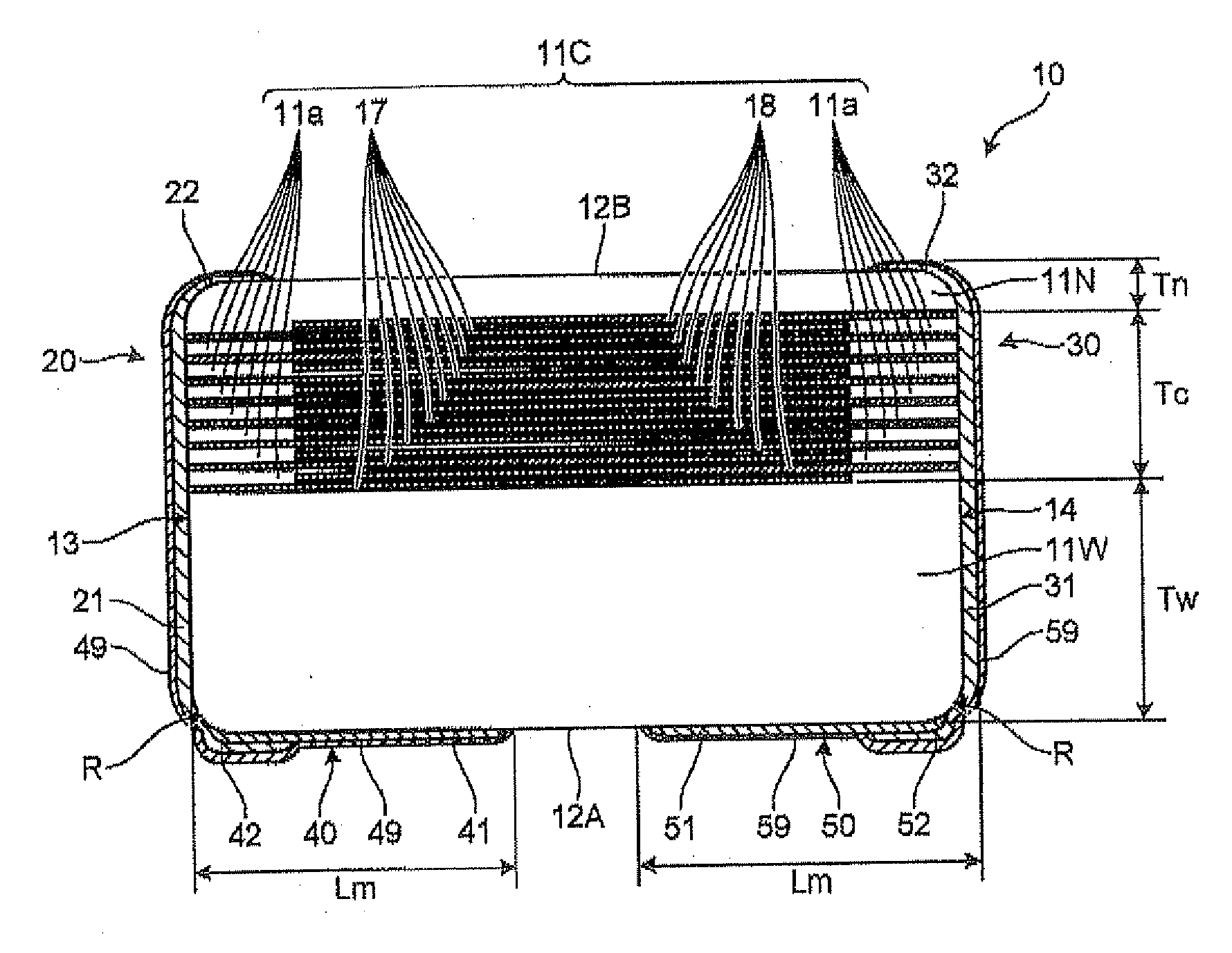
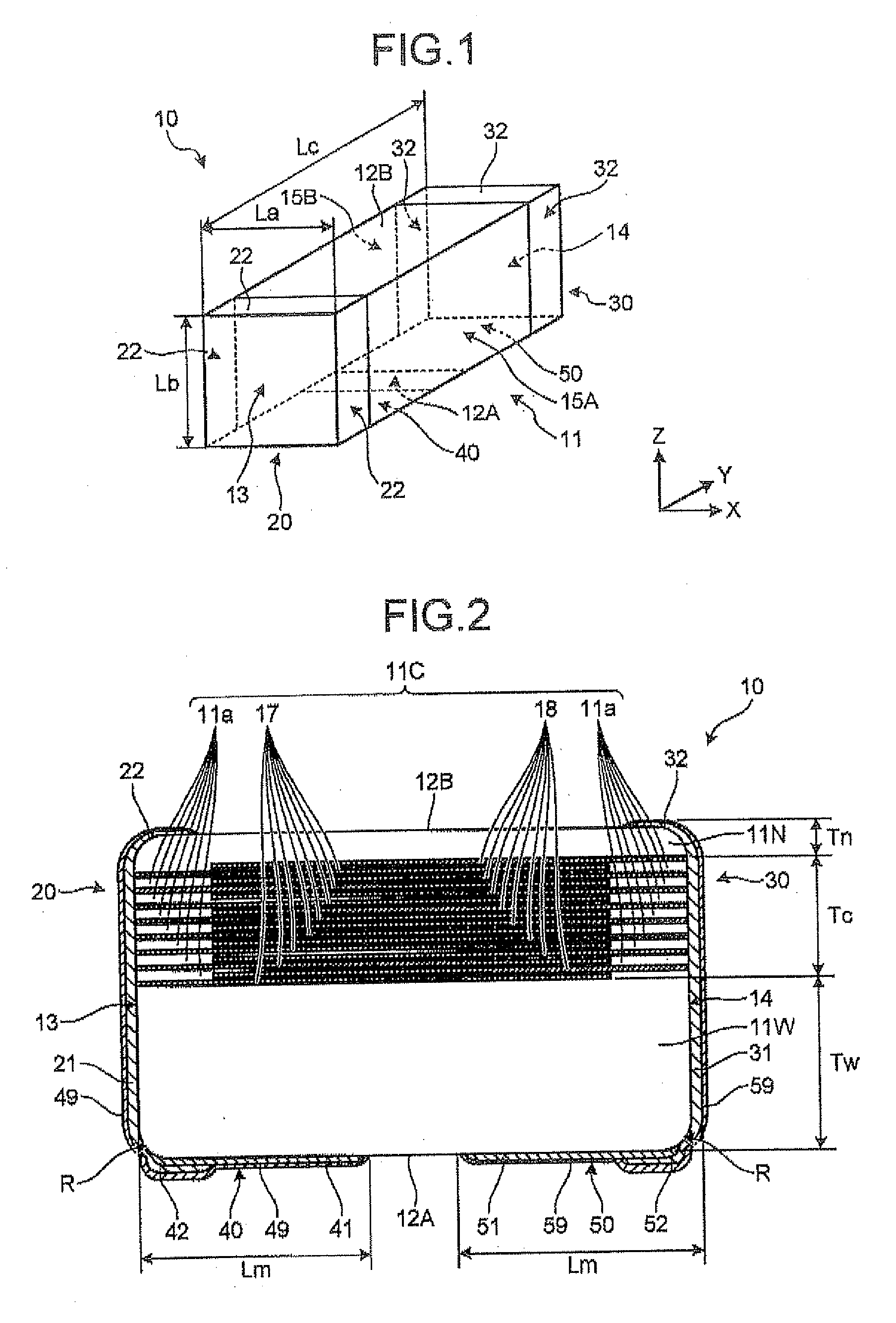
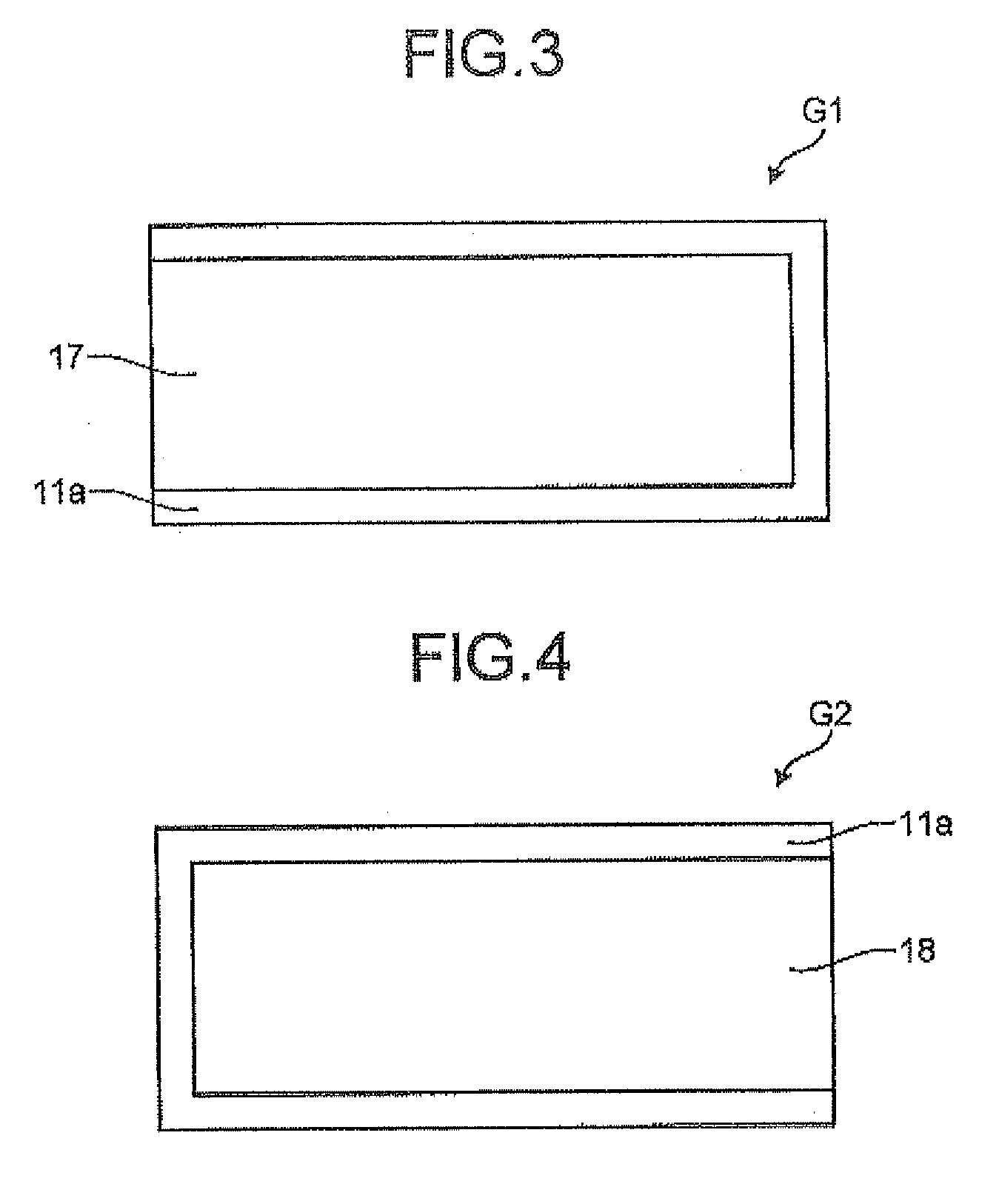
[0025]FIG. 1 is a perspective view showing a multilayer capacitor according to the present embodiment. FIG. 2 is a cross-sectional view showing the multilayer capacitor according to the present embodiment. FIG. 2 shows a cross-section of a multilayer capacitor 10 according to the present embodiment cut along a plane perpendicular to external electrode end face portions 21 and 31 of external electrodes 20 and 30 and internal electrodes 17 and 18. The multilayer capacitor 10 is a multilayer ceramic capacitor. The multilayer capacitor 10 includes a dielectric body 11, and the first external electrode 20 and the second external electrode 30 formed at end faces of the dielectric body 11. The multilayer capacitor 10 has a generally rectangular solid shape. Due to such a structure, the multilayer capacitor 10 includes a first body principal face 12A and a second body principal face 12B of the dielectric body 11 in a direction of stacking the internal electrodes 17 and 18 shown in FIG. 2 (s...

second embodiment

[0070]FIG. 10 is a perspective view showing a multilayer capacitor array according to the present embodiment. FIG. 11 is a perspective view showing an example of a dielectric body in the multilayer capacitor array according to the present embodiment. A multilayer capacitor array 10A according to the present embodiment is a multilayer capacitor including a plurality of internal electrode layered products 11C each interposed between a pair of the first dielectric layered product 11W and the second dielectric layered product 11N. In the following description, components same as those described in the first embodiment will be denoted by the same reference numerals, and a redundant description will be omitted.

[0071]For example, the multilayer capacitor array 10A includes three multilayer capacitors. The multilayer capacitors included in the multilayer capacitor array 10A each include external electrodes 20A and 30A, external electrodes 20B and 30B, and external electrodes 20C and 30C for...


PUM

PropertyMeasurementUnit
frequencyaaaaaaaaaa
conductiveaaaaaaaaaa
dielectricaaaaaaaaaa

Abstract

In a multilayer capacitor, a first dielectric layered product including a first body principal face is formed to be thicker than a second dielectric layered product including a second body principal face in a stacking direction thereof. A first external electrode and a second external electrode extend only to the first body principal face from a first body end face and a second body end face. Alternatively, the first external electrode and the second external electrode extend at least to the first body principal face from the first body end face and the second body end face and extend also to at least one of the second body principal face, a first body lateral face, and a second body lateral face.

Description

CROSS-REFERENCE TO RELATED APPLICATIONS[0001]This application is based upon and claims the benefit of priority from Japanese Patent Application No, 2011-117355, filed May 25, 2011, the entire contents of which are incorporated herein by reference.BACKGROUND OF THE INVENTION[0002]1. Field of the Invention[0003]The present invention relates to a multilayer capacitor to be mounted on a circuit board and a method for manufacturing the multilayer capacitor.[0004]2. Description of the Related Art[0005]An electronic device such as a personal computer, a PDA (personal digital assistant), or a mobile phone includes a circuit board on which a capacitor, an inductor, a varistor, or a composite component in combination thereof is surface-mounted. With such a structure, the entire circuit board in the electronic device is downsized by densely mounting electronic components thereon. Examples of the capacitor to be mounted on the circuit board may include a ceramic capacitor. Examples of the ceram...

Claims


Application Information

Patent Timeline
Patent Type & Authority Applications(United States)
IPC IPC(8): H01G4/30B32B37/14
CPCH01G4/30H01G4/232H01G4/12
Inventor TOGASHI, MASAAKI
Owner TDK CORPARATION
Why Eureka
Try Eureka