Managing apparatus of semiconductor manufacturing apparatus and computer program

a technology of semiconductor manufacturing and computer program, which is applied in the direction of program control, electric programme control, instruments, etc., can solve the problems of complicated and enlarged variation factors of the pattern to be formed, and achieve the effect of accurate specification of the exposure condition of the exposing devi

Inactive Publication Date: 2013-06-13
HITACHI HIGH-TECH CORP
View PDF11 Cites 2 Cited by
  • Summary
  • Abstract
  • Description
  • Claims
  • Application Information

AI Technical Summary

Benefits of technology

[0015]According to the above configuration, it is possible to perform a

Problems solved by technology

Accordingly, variation factors of the pattern t

Method used


Image

  • Managing apparatus of semiconductor manufacturing apparatus and computer program
  • Managing apparatus of semiconductor manufacturing apparatus and computer program
  • Managing apparatus of semiconductor manufacturing apparatus and computer program

Examples


Embodiment Construction

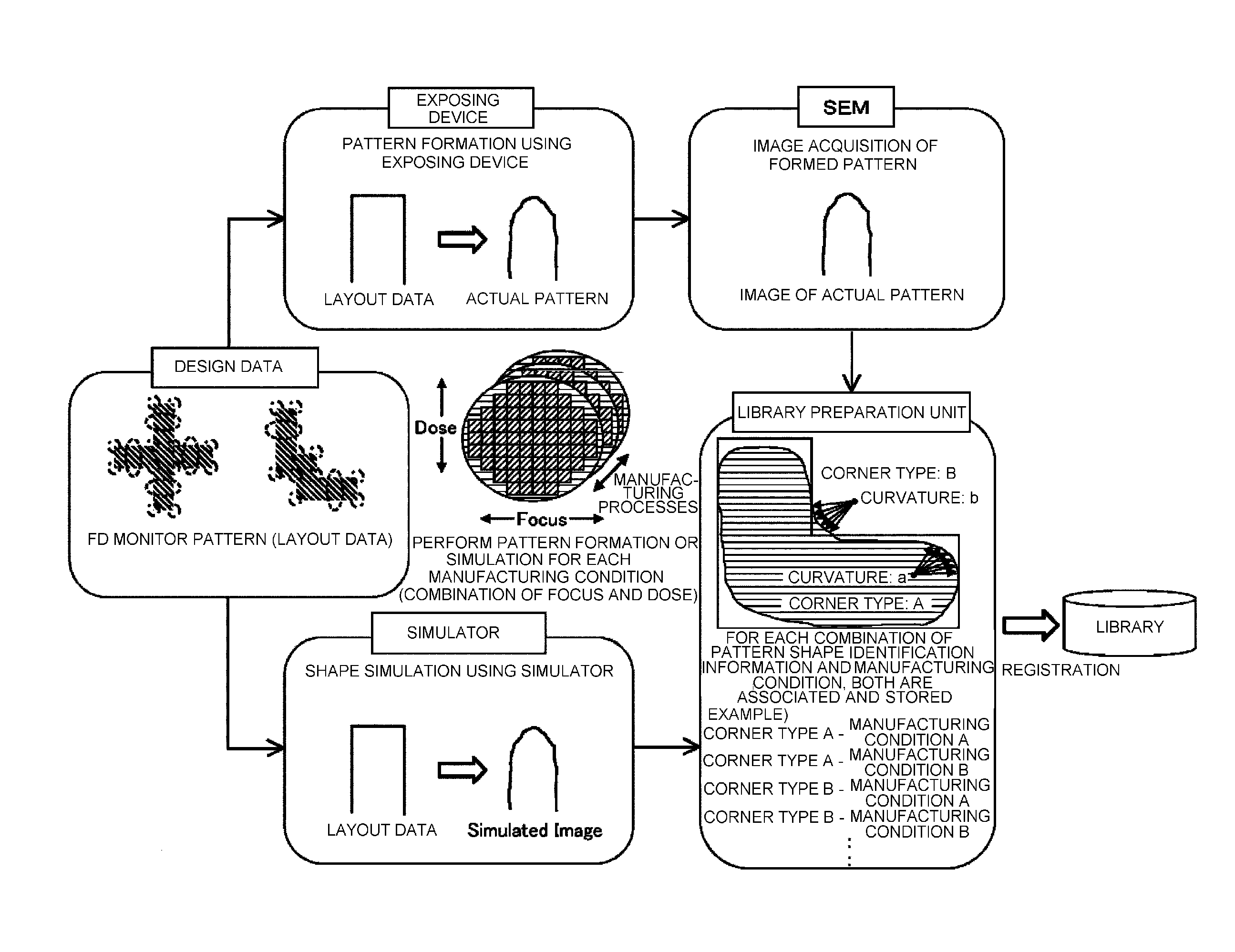
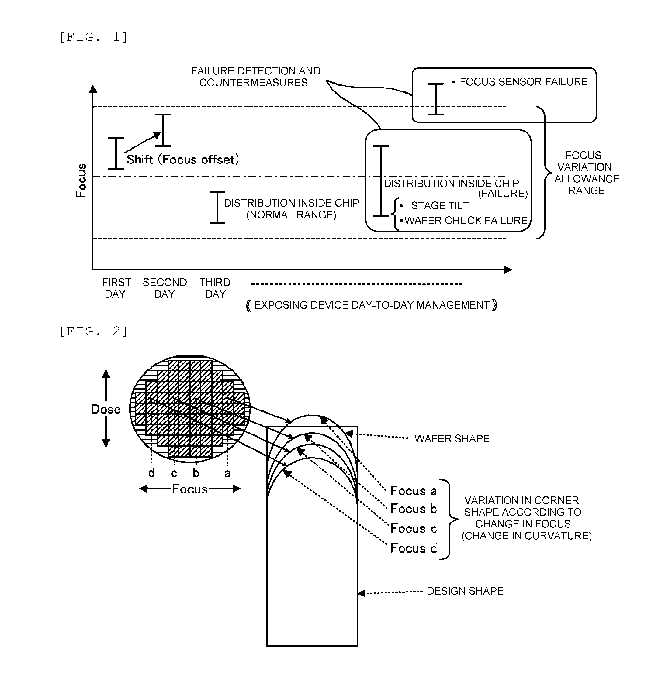
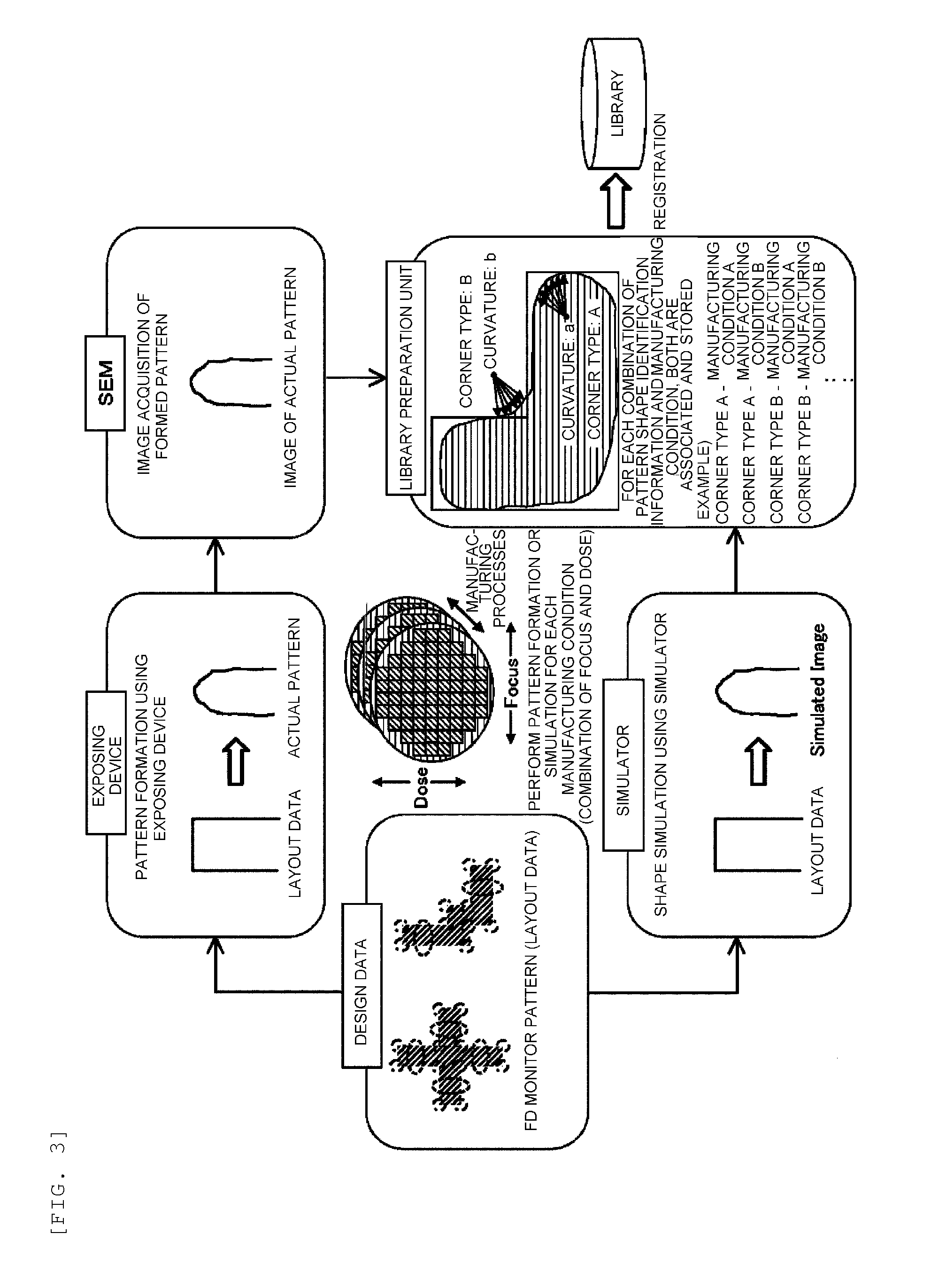
[0043]Inventors have newly discovered a phenomenon where due to an influence based on the variation in a focus value or an exposure amount, a big change occurs in shapes in corners of patterns (a connecting portion between two patterns having longitudinal directions in different directions, or the like) or a corner portion of a pattern (an apex angle portion). Therefore, in the present embodiment, a new managing apparatus of a semiconductor manufacturing apparatus and a computer program are proposed, in which the above portions are set as objects of shape evaluation, and a library which stores the association between the above portions and an exposure condition of an exposing device is prepared, thereby realizing a correct exposure condition by referring to the library.

[0044]Further, the inventors have newly discovered that, on design data, a plurality of parts having different angles, parts having the same angle but being present in different positions, and the like show a differen...


PUM


Abstract

An object of the present invention is to provide a managing apparatus of a semiconductor manufacturing apparatus and a computer program capable of performing an accurate process monitoring based on the obtained pattern image and the like. To accomplish the above object, according to one aspect of the present invention, there are proposed a managing apparatus of a semiconductor manufacturing apparatus including a library which stores an association between shape information of a pattern of a plurality of positions and an exposure condition of an exposing device and a calculation device which compares the shape information of the plurality of positions extracted from image information with the shape information stored in the library, and extracts the exposure condition based on a logical product of a range of a plurality of exposure conditions corresponding to the shape information of the plurality of patterns extracted from the image information, and a computer program which executes the above processes.

Description

TECHNICAL FIELD[0001]The present invention relates to a managing apparatus of a semiconductor manufacturing apparatus and a computer program to execute the management in a computer, and in particular, relates to a managing apparatus of a semiconductor manufacturing apparatus and a computer program which enable a process monitoring of an exposing device for exposing a semiconductor pattern.BACKGROUND ART[0002]Recently, according to progress of miniaturization technology in a manufacture of a semiconductor device, a pattern to be formed on a semiconductor wafer is miniaturized, so that an exposing device used for forming a pattern like this is requested to have a high NA (lens numerical aperture). Accordingly, variation factors of the pattern to be formed tend to be complicated and enlarged.[0003]Accordingly, it is necessary to always manage the state of the exposing device in the manufacturing process of the semiconductor. Whenever the exposing device has a failure, it is necessary t...

Claims


Application Information

Patent Timeline
IPC IPC(8): G05B19/418
CPCG03F1/70G03F7/705H01L22/12G05B19/4183H01L2924/0002G03F7/70625H01L2924/00
Inventor MATSUOKA, RYOICHIHASEGAWA, NORIOMITO, HIROAKI
Owner HITACHI HIGH-TECH CORP
Why Eureka
Try Eureka