Opto-electronic module and devices comprising the same

a technology of optoelectronic modules and optoelectronic modules, applied in the field of optoelectronics, can solve the problems of too large proximity sensors for certain applications, and achieve the effect of convenient and efficient (in particular wafer-level) manufacturing, simplified mounting and assembly of optoelectronic modules, and high precision

Active Publication Date: 2013-06-20
AMS SENSORS SINGAPORE PTE LTD
View PDF2 Cites 88 Cited by
  • Summary
  • Abstract
  • Description
  • Claims
  • Application Information

AI Technical Summary

Benefits of technology

[0018]Another object of the invention is to create a way of particularly safely detecting proximity.
[0129]Therein, one or more of the cases A) to D) and / or one or more of the cases e1) to e4) can be provided in order to accomplish this. And, this can make possible to achieve a predictable, safe operation of the opto-electronic module, wherein the opto-electronic module can even be particularly small. Cross-talk can be avoided or at least be largely reduced by this.

Problems solved by technology

It can be problematic to achieve a safe proximity detection, in particular when an energy-saving operation has to be ensured.
An furthermore, some proximity sensors are too large for certain applications.

Method used


Image

  • Opto-electronic module and devices comprising the same
  • Opto-electronic module and devices comprising the same
  • Opto-electronic module and devices comprising the same

Examples


Embodiment Construction

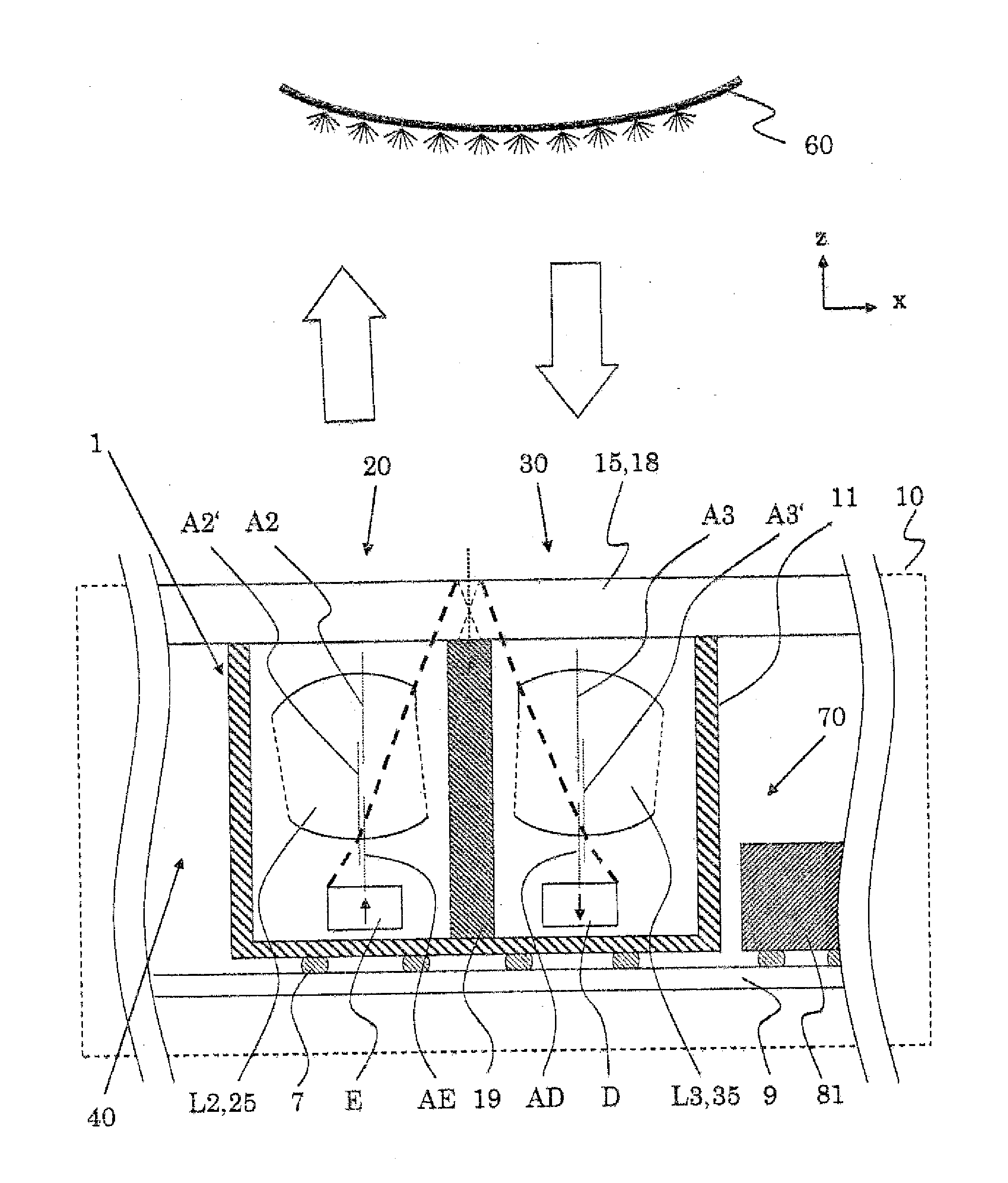
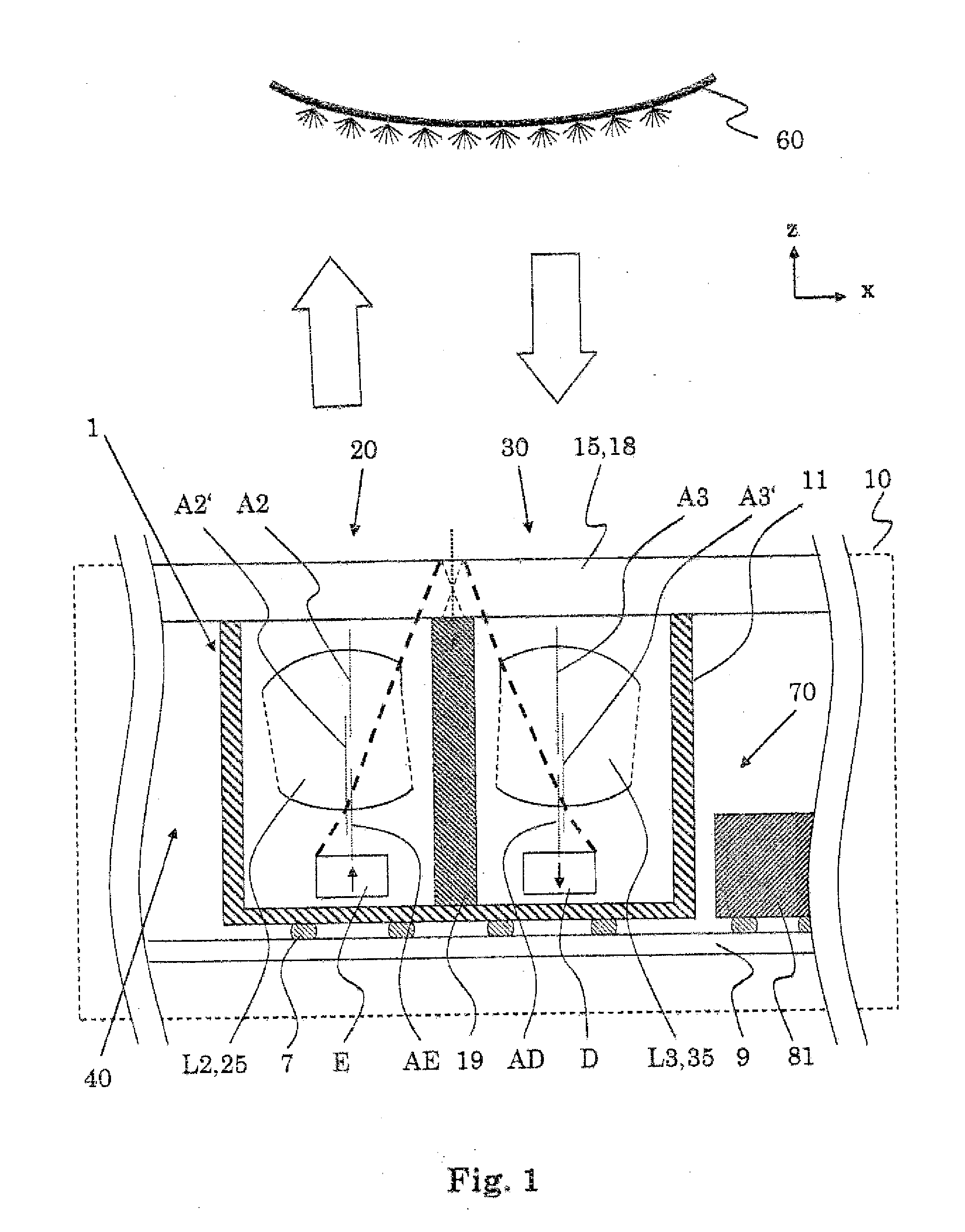
[0176]FIG. 1 shows a schematic cross-sectional illustration of an opto-electronic module 1, of an electronic circuit 70 comprising said opto-electronic module 1, of an electro-optic arrangement 40 comprising said opto-electronic module 1 and an object 18 and of a device 10 comprising said opto-electronic module 1 as well as said electronic circuit 70 and said electro-optic arrangement 40.

[0177]The device 10 is an electronic device and can in particular be a hand-held device, e.g., a hand-held music-playing device, a portable computing device, a photographic device, a mobile communication device, or others.

[0178]Device 10 comprises a housing 15, and, as illustrated in FIG. 1, it is possible to provide that opto-electronic module 1 is attached directly to housing 15, more specifically to that portion of housing 15 which is formed by object 18. Object 18 is at least partially transparent and is generally plate-shaped, at least on the region in which opto-electronic module 1 is attached...


PUM


Abstract

An opto-electronic module includes a detecting channel comprising a detecting member for detecting light and an emission channel comprising an emission member for emitting light generally detectable by said detecting member. Therein, a radiation distribution characteristic for an emission of light from said emission channel is non rotationally symmetric; and / or a sensitivity distribution characteristic for a detection in said detecting channel of light incident on said detection channel is non rotationally symmetric; and / or a central or main emission direction for an emission of light from said emission channel and a central or main detection direction for a detection of light incident on said detection channel are aligned not parallel to each other; and / or at least a first one of the channels comprises one or more passive optical components.

Description

CROSS-REFERENCE TO RELATED APPLICATIONS[0001]This application claims the benefit of priority of U.S. Provisional Patent Application No. 61 / 577,965, filed on Dec. 20, 2011, and U.S. Provisional Patent Application No. 61 / 699,687, filed on Sep. 11, 2012. The contents of the earlier applications are incorpoated herein by reference in their entirety.TECHNICAL FIELD[0002]The invention relates to the field of opto-electronics and more specifically to miniaturized opto-electronic components. More particularly, it relates to opto-electronic modules and to appliances and electronic devices comprising such modules, in particular wherein the modules comprise a light detector and a light emitter, more particularly wherein the modules comprise or are a proximity detector. The invention relates to apparatuses according to the opening clauses of the claims.DEFINITION OF TERMS[0003]“Active optical component”: A light sensing or a light emitting component. E.g., a photodiode, an image sensor, an LED,...

Claims


Application Information

Patent Timeline
Patent Type & Authority Applications(United States)
IPC IPC(8): G01J5/08G01S17/04
CPCG01S17/026G01S7/4811G01V8/12G01J1/0411G01J5/08G01S17/04
Inventor ROSSI, MARKUSKETTUNEN, VILLE
Owner AMS SENSORS SINGAPORE PTE LTD
Why Eureka
Try Eureka