Gated circuit structure with self-aligned tunneling region

a tunneling region and gate circuit technology, applied in the field of tunneling field effect transistors, can solve problems such as increasing process challenges

Inactive Publication Date: 2013-12-05
INTEL CORP
View PDF4 Cites 26 Cited by
  • Summary
  • Abstract
  • Description
  • Claims
  • Application Information

AI Technical Summary

Problems solved by technology

As microelectronic device size is continually scaled down, process challenges may increase.

Method used


Image

  • Gated circuit structure with self-aligned tunneling region
  • Gated circuit structure with self-aligned tunneling region
  • Gated circuit structure with self-aligned tunneling region

Examples


Embodiment Construction

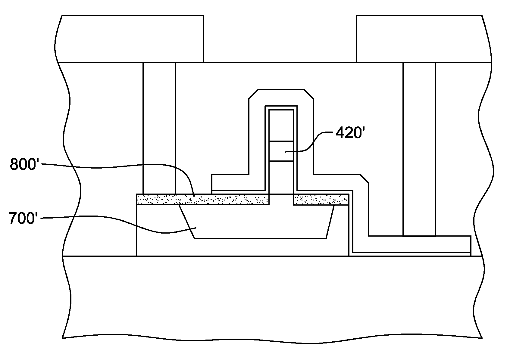
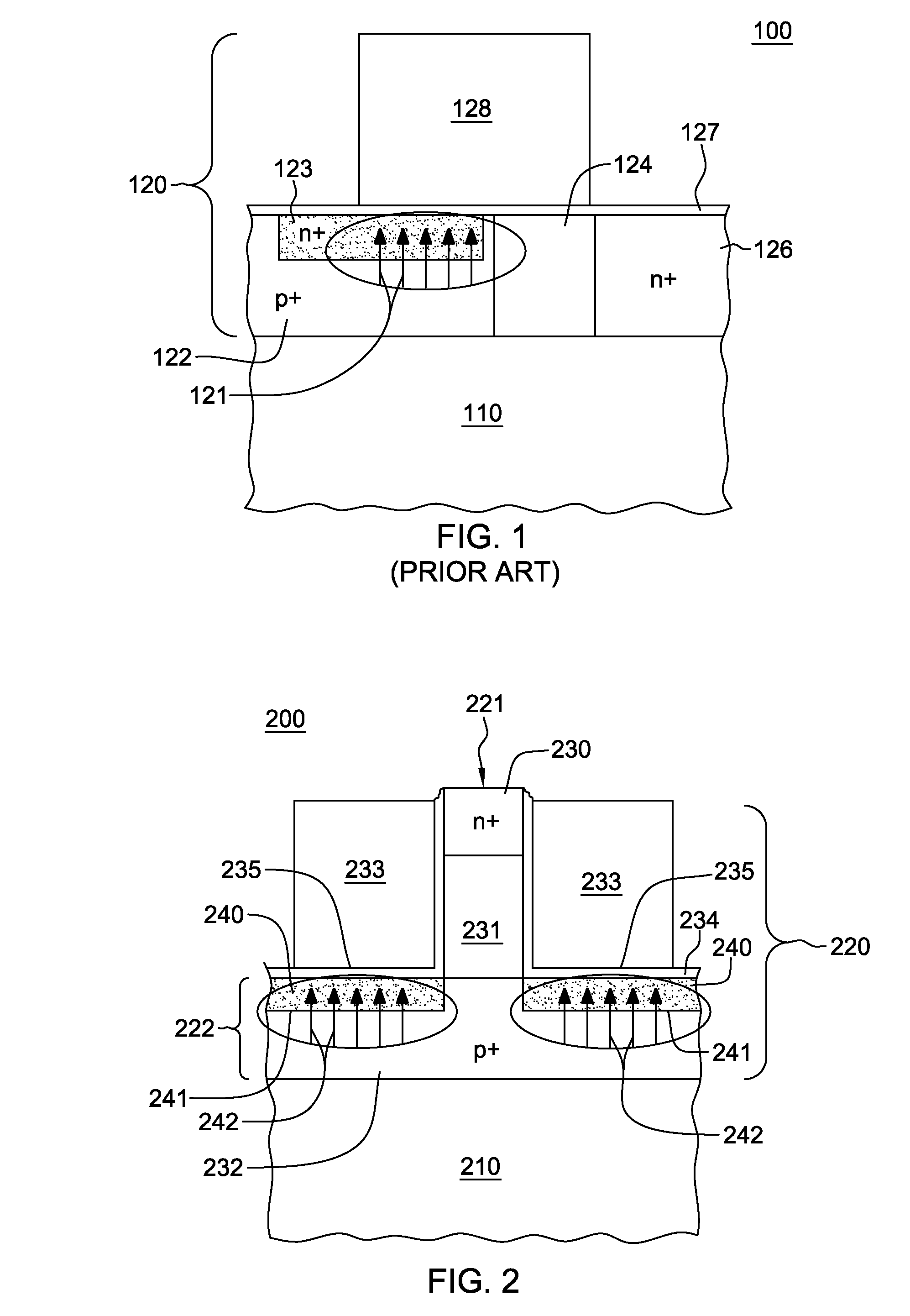
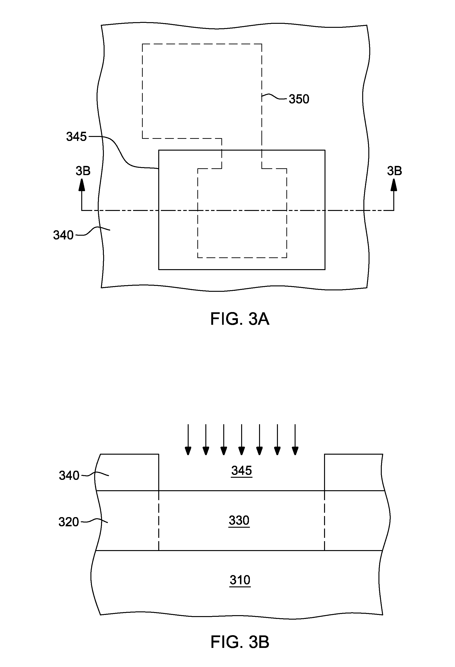
[0035]Generally stated, disclosed herein is a semiconductor device comprising a gated circuit structure, and a method of fabrication thereof. The gated circuit structure, which in one embodiment is a tunnel field-effect transistor (TFET), includes an angled circuit structure (such as a fin-shaped circuit structure or an L-shaped circuit structure), a gate electrode associated with the angled circuit structure, and a self-aligned tunneling region. The angled circuit structure is, in one embodiment, at least partially angled in cross-sectional elevation, and includes a first and second portion, with the first portion of the angled circuit structure extending away from the second portion thereof, for example, at a right angle. The self-aligned tunneling region is self-aligned to at least a portion of the angled circuit structure, and extends between the gate electrode and at least one of the first portion or the second portion of the angled circuit structure. Further, the self-aligned ...


PUM


Abstract

A tunnel field-effect transistor is provided, which includes a fin-shaped, source-drain circuit structure with a source region and a drain region. The circuit structure is angled in cross-sectional elevation, and includes a first portion and a second portion. The first portion extends away from the second portion, and the source region is disposed in the first or second portion, and the drain region is disposed in the other of the first or second portion. The transistor further includes a gate electrode for gating the circuit structure and a self-aligned tunneling region. The tunneling region is self-aligned to at least a portion of the circuit structure and extends between the gate electrode and the first or second portion of the fin-shaped circuit structure, and the self-aligned tunneling region is at least partially disposed in parallel, spaced opposing relation to a control surface of the gate electrode.

Description

BACKGROUND[0001]This invention relates generally to semiconductor devices, and to processes for making semiconductor devices, and more particularly, to tunnel field-effect transistors and methods of making the same.[0002]The sizes of microelectronic devices and other active and passive electrical components are continuously scaled down in attempts to increase device integrated-circuit density. Field-effect transistors are fabricated to provide logic and data-processing functions, among others, for the microelectronic devices built on a wafer. Typically, lithography techniques are used to define the sizes of the field-effect transistors in the devices. As microelectronic device size is continually scaled down, process challenges may increase.BRIEF SUMMARY[0003]The present invention relates, in one aspect, to a semiconductor device which includes a gated circuit structure. The gated circuit structure comprises an angled circuit structure, a gate electrode, and a self-aligned tunneling...

Claims


Application Information

Patent Timeline
Patent Type & Authority Applications(United States)
IPC IPC(8): H01L29/78H01L21/283
CPCH01L29/66356H01L29/7391
Inventor LOH, WEI-YIPHILL, RICHARDMAJHI, PRASHANT
Owner INTEL CORP
Why Eureka
Try Eureka